Switch project, part 3 - what Microchip doesn't (officially) tell you about the VSC8512
2025-07-04 08:00This is part 3 of my ongoing series about LATENTRED, my project to create an open source 1U managed Ethernet switch from scratch.
Here’s a quick, or maybe not-so-quick, update about the PHY on the line card and some of my troubles (and solutions).
And probably more internal details than you want to know, but hey - maybe this will be useful to somebody. Not a lot of pretty pictures either. One day I do want to decap one for fun, but I have better things to do with my time than try to fully netlist-extract a large 65nm IC just to figure out some undocumented registers.
Background
I chose the VSC8512 as the PHY for the line card because it had a QSGMII interface (which used much less pins than SGMII), but also (so I thought) had a fully open datasheet with no NDAs required.
Typically I’m used to seeing parts that are either fully NDA’d (with a trivial product brief and no register info etc, or sometimes not even pinout info, public), or fully open. Sometimes I find components with specific documents restricted, but it’s almost always clear that “this document/ref design exists, you can’t get it without an NDA, but we are openly telling you we’re holding it back”.
In my previous post I mentioned that there was no documentation for how to change the SERDES TX equalizer settings on the PHY side of the QSGMII. I opened a support case and Microchip responded saying that additional info was available in the “confidential reference manual” for the part which required an NDA. The rest of the reply was pretty generic and mentioned indirect register access but no specifics.
I was quite annoyed at this, as I had specifically chosen the part believing there was no restricted documentation. Since signing an NDA wasn’t an option, it seemed I had the choice of suboptimal signal integrity or figuring things out from the limited public information. The eye was still reasonably open as-is and my cables and boards didn’t have a ton of insertion loss, so worst case things would probably work with the default TX config.
But why would I settle for bad SI when I could read a bunch of poorly documented code and datasheets deliberately missing details?
What we have to go on
So, we know there is a confidential reference manual. But there’s a lot of docs available to the public - after all, I was able to make a board, bring up the PHY, and pass packets without it.
- VSC8512 datasheet (VMDS-10396). This is 139 pages of meat including what I thought was a complete set of registers.
- VSC8512 hardware design checklist (DS00004697A)
- VSC8504 Serdes6G IBIS-AMI model. This is for the 4-port version of the same PHY but is linked on the product web page; presumably the 04 and 12 use the same IP.
- VSC742x / 85x2 reference design guide (UG1037). This describes a 24-port switch reference design using a SparX-III / Caracal switch ASIC (including 12 integrated PHYs) paired with a VSC85x2. Not a ton interesting here.
- Microchip Ethernet Switch API (MESA), MIT licensed HAL for Microchip/Vitesse PHYs and switches available on GitHub. As you’ll see in a bit, this is an absolute gold mine of information but it’s (perhaps intentionally) not well documented what a lot of the bitfields and APIs do.
Initial observations
It’s pretty easy to see that the VSC8512 is a nerfed switch ASIC. There’s an entire DDR I/O controller that’s unused (over a dozen VDD_IODDR pins you’re instructed to ground, plus a large group of NC pins in the surrounding area). So docs for the un-crippled switch ASIC, which I suspected and later confirmed was the VSC742x, are potentially of interest too.
The IBIS-AMI model included the magic name “Serdes6G”. Searching for this turned up some additional docs, most notably AN3743 (DS00003743A) which purports to be about the VSC74xx / 84xx but seems to be describing something very similar to what’s on the 8512.
Between the various documents I was able to conclude that the VSC8512 is made on an unspecified 65nm process (I should decap one at some point and figure out whose / see what it looks like… Luton first stepping is mentioned as being fabbed at TSMC in vtss_phy_do_page_chk so I suspect the rest are as well).
The SERDES macro was developed by the “German Design Center” (in the Dortmund area, according to some LinkedIn hits from a google search) - interesting to know, but not particularly useful in this context.
The IBIS model describes some very useful parameters. We don’t know how to actually set them yet, but we know they exist, their ranges, and (most importantly) their names:
OB_LEV: amplitude / main cursor tap, 0 to 63OB_PREC: pre-cursor FFE tap, -15 to +15OB_POST0: post cursor 0 FFE tap, -31 to +31OB_POST1: post cursor 1 FFE tap, -15 to +15OB_POL: output invertOB_SER_H: coarse slew rate adjust (slow/fast)OB_SER: fine slew rate adjust, 0 to 15
These were all critical key words to look for elsewhere in docs and code, and ultimately put me on the track of success.
Of note is that this SERDES offers more knobs on the output driver than most: slew rate control is rare on IOs of this class (most just run as fast as possible all the time), and most TX FFEs only have a single post-cursor tap, while this one has two.
MESA is not super well documented, you have to know what you’re looking for. But there’s a ton of detail once you do.
I already knew that the relevant PHY driver code in MESA was in mepa/vtss/src/phy_1g. The relevant files are vtss_phy.* (main driver) and vtss_phy_init_scripts.* (sequences of canned register writes for configuration in various modes and working around silicon bugs in old silicon steppings).
I had previously looked at the PHY init scripts and grabbed the important register settings out of them for a few things. There was also a microcode patch for an internal 8051 MCU (good to know this exists!) however I didn’t include the microcode patch in my firmware because the D stepping (rev 0x3) of the VSC8512, the only one you can still get, has fixes for most of the errata the patch fixes other than something in 100baseFX mode that I don’t care about.
vtss_phy.h has an enum with a bunch of different device families and the VSC8512 is mentioned in a comment as being VTSS_PHY_FAMILY_ATOM. Comments elsewhere refer to it at Atom12. Luton26, Viper, and Elise appear to be very similar as most switch statements take the same path for these parts; Tesla and Nano are also close relatives. The VSC8504 is a Tesla, interestingly - not an Atom - but seems to use the same SERDES or a very close version.
The initialization scripts are in a function called luton26_atom12_revCD_init_script which suggests Luton26 and Atom12 are register and bug-for-bug compatible for most configuration. This makes sense, since Luton26 is the VSC742x and I already suspected Atom12 was a nerfed PHY-only version of the same platform for other reasons (identical pinouts, etc).
This adds VMDS-10393, the VSC742x datasheet, to our reading list as something potentially worth looking at.
Interestingly, the VSC742x has a MIPS core not an 8051. It’s possible the comments are wrong and this isn’t actually an 8051 (I didn’t try disassembling the microcode patch); it’s also possible that there is an 8051 core that’s separate from the MIPS. Maybe in the PHY fuse configuration of the die, the MIPS is disabled and the 8051 provides all of the minimal management infrastructure from a ROM or something.
Known register interfaces
The VSC8512 responds to 12 consecutive MDIO addresses, one per PHY (base address selected by strap pins). On the LATENTRED line card, one PHY is mapped at MDIO address 0-11 and the second at 12-23. Some operations are global and should be addressed to PHY 0 within the device, while others are per-PHY and should be addressed to the appropriate port index.
The VSC8512 has three separate documented register interfaces, all accessed via MDIO (there’s one more that we’ll get to later).
- The IEEE standard MDIO register space from 0x00 to 0x0f. This works as you’d expect with any other PHY.
- IEEE standard indirect MMD register access using registers 0xd and 0xe. This works as you’d expect, but is only used for accessing five registers for EEE (energy efficient Ethernet).
- Vendor defined registers, selected by a page/bank index in register 0x1f. Note that the bank selector remaps the entire 31-register address space, i.e. when the page selector is not 0x0000 the IEEE standard registers are not available.
There are five documented pages and two known undocumented ones.
Page 0x0000: Base / Main (datasheet 5.1 / 5.2)
There seems to be a formatting error in the doc (somebody accidentally made register 0x17 a level 2 heading instead of level 3) so the PDF ToC and section numbering is borked.
This page includes the IEEE standard registers and some vendor specific ones related to baseT extended status and error detection.
Other features and tidbits of note:
- Chicken bits in register 0x12 for things like disabling MDI-X, bypassing the 100baseTX 4b5b coder, and disabling a workaround for problems when the device is paired with a specific old Broadcom PHY.
- Error counters in 0x13 - 0x15 for detecting various link faults
- SFP vs baseT selectors in 0x17
- Jumbo frame enable in 0x18
- Interrupt control and status in 0x19 / 0x1a
- Auxiliary control/status in 0x1c. This lets you detect things like MDI vs MDI-X state, pair swap, polarity inversion, etc. It also provides fields containing duplex and speed state duplicating those in IEEE standard register 0, but reporting the actually negotiated speed/duplex. (Fun tidbit, register 0 readback is not well defined in the spec! Some PHYs like the KSZ9031 let you read back the current negotiated state, while others like the VSC8512 always read the last value written)
Page 0x0001: Extended 1 (datasheet 5.3)
This page mostly has config for the low speed (1 Gbps) SERDES used for gigabit SFP applications. I’m not using these on the switch, so I’m pretty much ignoring them.
There’s also a built in test pattern packet generator in register 0x1d/1e which is cool, although since I’m driving the PHYs from an FPGA I’d rather build my own test pattern generator in fabric so I can seed them with a PRBS or something to make validation easier.
Page 0x0002: Extended 2 (datasheet 5.4)
This page contains some fine-tuning registers for adjusting baseT signal amplitude and linearity to compensate for performance of various magnetics. If/when I end up doing full 1000baseT signal quality compliance (this would be a nice feature to add to ngscopeclient eventually) I’ll likely use these.
There’s also a few other miscellaneous settings related to EEE.
Page 0x0003: Extended 3 (datasheet 5.5)
This page contains config and status related to the serial MAC interface (SGMII / QSGMII). Note that actual SERDES PHY controls such as equalizers and inversion are not here.
Page 0x0010: GPIO / MCU (datasheet 5.6)
This page is a fun one.
There’s a bunch of “boring” registers related to the GPIO pins, an I2C mux intended for external SFPs, recovered clock debug outputs, etc.
But… there’s also register 0x12 which is basically a mailbox to the internal MCU. We’ll be talking a lot more about this later on, but there’s lots of fun to be had here.
Page 0x2a30: Test (undocumented)
I have no idea what this does, it’s not mentioned in the datasheet at all and the code has no comments or details whatsoever. Probably chicken bits. I haven’t tried poking any of the values to see if I can see any difference in behavior.
MESA has a function luton26_atom12_revCD_init_script that writes the following values:
- 0x14 = 0x4420
- 0x18 = 0x0c00
- 0x9 = 0x18c8
- 0x8: set MSB, leave other bits unchanged
- 0x5 = 0x1320
- After rest of init, clear MSB of 0x8
Page 0x52b5: Token Ring / black magic (undocumented)
No idea what this does either. Datasheet doesn’t mention it, most MESA code just calls it TR, but a few bits call it Token Ring.
I can’t imagine that is correct, there’s no reason for a 1984-era protocol to be present in a modern Ethernet PHY. Maybe somebody saw the acronym and filled it in wrong? IDK.
Anyway, the PHY init script has a big block of triplet writes to 0x12, 0x11, 0x10, always in that order. No comments or clues as to what it does, other than that 10baseT vs 10baseTe mode require a different sequence in one spot, and the final write is commented as “Improve 100BASE-TX link startup robustness to address interop issue”.
Guessing these are chicken bits of some sort too, but who knows.
EDIT: vtss_phy_optimize_receiver_init mentions some stuff about registers called half_comp_en and half_adc. There’s also some stuff in vtss_phy_power_opt that someone might want to dig into eventually. Seems to be some sort of link training to save power by reducing TX amplitude or something? vtss_phy_optimize_receiver_reconfig talks about vga_state as well.
Very rough conjecture and not tested in the slightest:
- 0x12: read pointer
- 0x11: read/write data register
- 0x10: write pointer
vtss_phy_debug_tr_regdump_print may also be worth looking at, it suggests that 0x10 might be a read pointer too?
MCB (Macro Configuration Bus)
The VSC742x datasheet goes into a little more detail about this - basically it’s a separate bus used for configuring the SERDES6G.
There’s no direct access to the MCB on the VSC8512 from the outside. Instead, you issue a command to the MCU to read all MCB registers from a SERDES macro into a working buffer (“PRAM”, “cfg_buf”, or “shadow registers”), use peek/poke commands to manipulate this buffer, then issue another command to write it back to one or more SERDES macros.
Understanding the MCU interface
So now we’re back to trying to understanding the MCU interface a bit more to try and figure out how to do fun things with it (and to solve my original problem of configuring the equalizer).
Starting with the SERDES register field names, most notably post0 as this is the one I care about the most (the first post cursor tap provides de-emphasis to open the eye up) I started searching through the MESA code for anything that looked relevant.
There’s a function vtss_phy_cfg_ob_post0 in vtss_phy_1g_api.h, with an accurate-ish yet useless comment “Debug function for setting the ob post0 patch”. You’d never know what this did from the prototype or comment if you didn’t dig as deep into the platform as I had, although looking at the source and seeing some of the implementation gated behind a #ifdef VTSS_FEATURE_SERDES_MACRO_SETTINGS might give a hint. Interestingly another part of the headers say “do not change” the post1 tap from the power-on default of zero, perhaps there’s a silicon bug around this?
This function does some minimal error checking, then calls vtss_phy_cfg_ob_post0_private which has a slightly less useless comment “Function to set the ob_post0 parameter after configuring the 6G macro for QSGMII for ATOM12”. After some more validation and checking that we are in fact on an Atom12 (there’s a separate code path for Tesla)…
It just does a big pile of reads and writes to register 0x12 in the GPIO/MCU page, aka register “18G”, “Global Command and SerDes Configuration”, or VTSS_PHY_MICRO_PAGE depending on where you look.
So what is it? All we have is a single 16-bit register (inside of the proprietary extended MDIO register window scheme, but we’ll forget about that for the time being). Can’t be that complicated.
Instruction formats
Bit 15 is actually documented: set high to execute a command, poll for it to self clear before doing anything else.
After some digging through vtss_phy.c and the VSC8512 datasheet, I made some progress. There’s actually two different instruction word formats for the remaining bits.
Bit 14 set: Indirect pointer format
This instruction sets a 15-bit pointer mem_addr into the MCU memory address space used by peek/poke commands.
[15]: always 1 (execute command)[14]: always 1 (select indirect pointer mode)[13]: always 0 (seems to be dontcare)[12]: segment / base address select (1 = 0x4000, 0 = 0x0000)[11:0]: low bits of pointer
Bit 14 clear: Command format
This instruction executes a command and optionally returns data.
[15]: always 1 (execute command)[14]: always 0 (select command mode)[13:4]: arguments, opcode dependent[3:0]: opcode
Command codes
0x0: Set MAC mode / write MCB to shadow registers
Two commands are documented in datasheet table 77:
80b0: select 12 phy SGMII mode80a0: select 12 phy QSGMII mode
One undocumented command is known from MESA:
9cc0: write shadow registers fromcfg_bufto one or more MCB ports selected by theaddr_vecbitmask. There’s probably some bitfields to crack here (maybe related to 0x03 command syntax)? to access other stuff.
It looks like Tesla uses 80e0 for QSGMII mode but I haven’t seen this used in any of the Atom12/Luton26 code.
0x1: Set SERDES media mode for dual mode SFP/baseT interfaces
Two commands are documented in datasheet table 77:
[15]: always 1 (execute command)[14]: always 0 (select command mode)[13:12]: always 0 (reserved/ignored?)[11:8]: bitmask of port 11:8 indexes, 1 to set mode, 0 to preserve[7:4]: 0x8 for 1000baseX, 0x9 for 100baseFX, other values reserved[3:0]: opcode (always4'h1)
0x2: Unknown, not observed
0x3: Read MCB to shadow registers
One undocumented command is known from MESA. This command reads the entire 36 byte MCB from a single SERDES macro into a variable called cfg_buf, located in the 8051 memory at address 0x47cf.
[15]: always 1 (execute command)[14]: always 0 (select command mode)[13:12]: always 0 (reserved/ignored?)[11:8]: SERDES macro index on the specified MCB, see below[7:4]: MCB bus index, see below[3:0]: opcode (always4'h3)
MCB bus indexes for the VSC8512:
- 0: SERDES1G macros
- 1: SERDES6G macros
- 2: LCPLL
SERDES1G macro indexes on MCB bus 0:
- 0: SERDES1G macro 0 (SGMII lane 1)
- 1: SERDES1G macro 1 (SGMII lane 2)
- 2: SERDES1G macro 2 (SGMII lane 4)
- 3: SERDES1G macro 3 (SGMII lane 5)
- 4: SERDES1G macro 4 (SGMII lane 7 / SFP port 11)
- 5: SERDES1G macro 5 (SGMII lane 8 / SFP port 10)
- 6: SERDES1G macro 6 (SGMII lane 10 / SFP port 9)
- 7: SERDES1G macro 7 (SGMII lane 11 / SFP port 8)
SERDES6G macro indexes on MCB bus 1:
- 0: SERDES6G macro 0 (SGMII lane 0 / not used for QSGMII)
- 1: SERDES6G macro 1 (SGMII lane 3 / QSGMII lane 0)
- 2: SERDES6G macro 2 (SGMII lane 6 / QSGMII lane 1)
- 3: SERDES6G macro 3 (SGMII lane 9 / QSGMII lane 2)
0x4: Suspend 8051 patch
This disables updated 8051 firmware (and I guess reverts to the ROM version) temporarily.
[15]: always 1 (execute command)[14]: always 0 (select command mode)[13:12]: always2'b01[11:4]:8'h01to suspend microcode,8'h0to resume[3:0]: opcode (always4'h4)
0x5: Unknown, not observed
0x6: Byte poke
This writes a single byte at mem_addr on the 8051.
[15]: always 1 (execute command)[14]: always 0 (select command mode)[13]: always 0 (reserved/ignored?)[12]: if 1,mem_addris incremented after the poke. if 0,mem_addris unchanged[11:4]: byte to write tomem_addr[3:0]: opcode (always4'h6)
0x7: Byte peek
This reads a single byte from mem_addr on the 8051.
Write format:
[15]: always 1 (execute command)[14]: always 0 (select command mode)[13]: always 0 (reserved/ignored?)[12]: if 1,mem_addris incremented after the peek. if 0,mem_addris unchanged[11:4]: always 0 (reserved/ignored?)[3:0]: opcode (always4'h7)
Result readback format:
[15]: busy bit, poll until zero[14:12]: reserved, ignore[11:4]: byte read from MCU memory[3:0]: reserved, ignore
0x8 - 0xc: Unknown, not observed
0xd: Squelch workaround
Not sure what this does, it seems only implemented or necessary in Tesla / Viper parts but noted here to explain the hole in the opcode space
0xe: Unknown, not observed
0xf: Unimplemented / nop
This is used in some pieces of the code such as vtss_atom_patch_suspend to temporarily disable the 8051 EEE microcode patch during TDR testing because apparently issuing an unimplemented command makes the patch suspend. Why not use command 0x4? Who knows.
Per comment in the code “Note that this is necessary only because the patch for EEE consumes the micro continually to service all 12 PHYs in a timely manner and workaround one of the weaknesses in gigabit EEE in Luton26/Atom12.”
MCU address space
I have not yet attempted to read or mess with most of the 8051 address space.
From looking at MESA, the following addresses, names, and values are known (this is not all inclusive, just what I’ve looked at). These appear to correlate with the bitfield names in SERDES6G_ANA_CFG in vtss_phy.h. While the macro names refer to Tesla, looking at the code it appears Tesla uses the same or very similar SERDES as Luton26/Atom12 so it’s very likely that all of these field names map directly.
47cb / name unknown
Seems related to SERDES loopback, see vtss_phy_serdes_fmedia_loopback_private
47ce / addr_vec
Bitmask of SERDES6G macros to write shadow registers back to when sending 9cc0 command.
[7:4]: reserved, write as zero[3:0]: write enable mask for SERDES6G lanes 3:0. 1=write, 0=ignore
47cf / cfg_buf[0] / cfg_vec[7:0]
Unknown
47d0 / cfg_buf[1] / cfg_vec[15:8]
Unknown
47d1 / cfg_buf[2] / cfg_vec[23:16]
Unknown
47d2 / cfg_buf[3] / cfg_vec[31:24]
[7:5]: unknown[4]: facility loopback in QSGMII mode if I’m reading code right? header calls itVTSS_TESLA_SERDES6G_ANA_CFG_PWD_TX_6G)[3:0]: unknown
47d3 / cfg_buf[4] / cfg_vec[39:32]
Unknown
47d4 / cfg_buf[5] / cfg_vec[47:40]
Unknown
47d5 / cfg_buf[6] / cfg_vec[55:48]
Unknown
47d6 / cfg_buf[7] / cfg_vec[63:56]
Unknown
47d7 / cfg_buf[8] / cfg_vec[71:64]
Unknown
47d8 / cfg_buf[9] / cfg_vec[79:72]
[7:5]: low 3 bits ofob_post0, output buffer postcursor 0 tap[4:0]: unknown
47d9 / cfg_buf[10] / cfg_vec[87:80]
[7]: unknown[6]:ib_rst[5:3]: unknown[2:0]: high 3 bits ofob_post0, output buffer postcursor 0 tap
47da / cfg_buf[11] / cfg_vec[95:88]
See vtss_phy_atom12_cfg_ib_cterm_ena_private
[7:4]: unknown[3]:ib_cterm_ena[2]:ib_eq_mode[1:0]: unknown
Other cfg_buf
According to vtss_phy_atom12_patch_setttings_get_private (note the typo), the cfg_buf array is 36 bytes long, while it’s 38 on Tesla. So maybe VTSS_TESLA_SERDES6G_DIG_CFG_PRBS_SEL_6G and higher registers are unavailable on Atom12?
Registers and fields mentioned in passing in the code worth digging into:
ob_cfg0:
ena1v_modeob_polob_post0ob_post1ob_sr_hob_resistor_ctrob_sr
ob_cfg1:
ob_ena_casob_lev
des_cfg:
phy_ctrlmbtr_ctrlbw_hystbw_ana
ib_cfg0:
ib_rtrm_adjib_sig_det_clk_selib_reg_pat_sel_offsetib_cal_ena
ib_cfg1:
ib_tjtagib_tsdetib_scalyib_frc_offset
ib_cfg2:
ib_tinfvib_tcalvib_ureg
ib_cfg3: mentioned, didn’t look at in any detail
ib_cfg4: mentioned, didn’t look at in any detail
47f3 / stat_buf
8 bytes long, no other details reversed.
Digging in vtss_phy_chk_serdes_init_mac_mode_private will probably shed light on variables sys_rst, ena_lane, pll_fsm_ena, hrate, qrate, if_mode, ib_fx100_ena, des_cpmd_sel, des_100fx_cpmd_ena but I haven’t spent any time on this.
vtss_serdes6g_tesla_rcpll_status_get_private suggests the following fields for the RC PLL (SERDES1G?):
- bit 10:
out_of_range - bit 11:
cal_error - bit 12:
cal_not_done
vtss_lcpll_tesla_status_get_private suggests the following fields for the LC PLL (SERDES6G?):
- bit 45:
lock_status - bit 36:
cal_done - bit 35:
cal_error - bit 32:
fsm_lock - bit 31:29:
fsm_stat - bit 18:14:
gain_stat
QSGMII equalizer testing
So, with all that, where does that leave us?
I now know how to tune at least the critical post-cursor tap 0 to do basic de-emphasis:
- Read MCB registers from SERDES lane 1 (first QSGMII lane) with
0x03command into shadow regsters - Poke
ob_post0using the indirect access command to set the pointer followed by a pair of0x07/0x06peek / poke operations to read-modify-write this field without changing others - Poke addr_vec to
0x0eto select all three of the four total SERDES6G lanes that are used for QSGMII - Send
0x9cc0command to push the new register values to all SERDES instances
I’m on the edge of figuring out a lot more by guessing what the bitfield names in the header mean (this post is in part my notes in case I want to get back to this and tune other configuration like output amplitude).
With the default post0 tap value (I believe 0x02 from MESA comments, but have not actually tried to read back) the signal is totally usable, but there is just a smidgeon of eye closure.
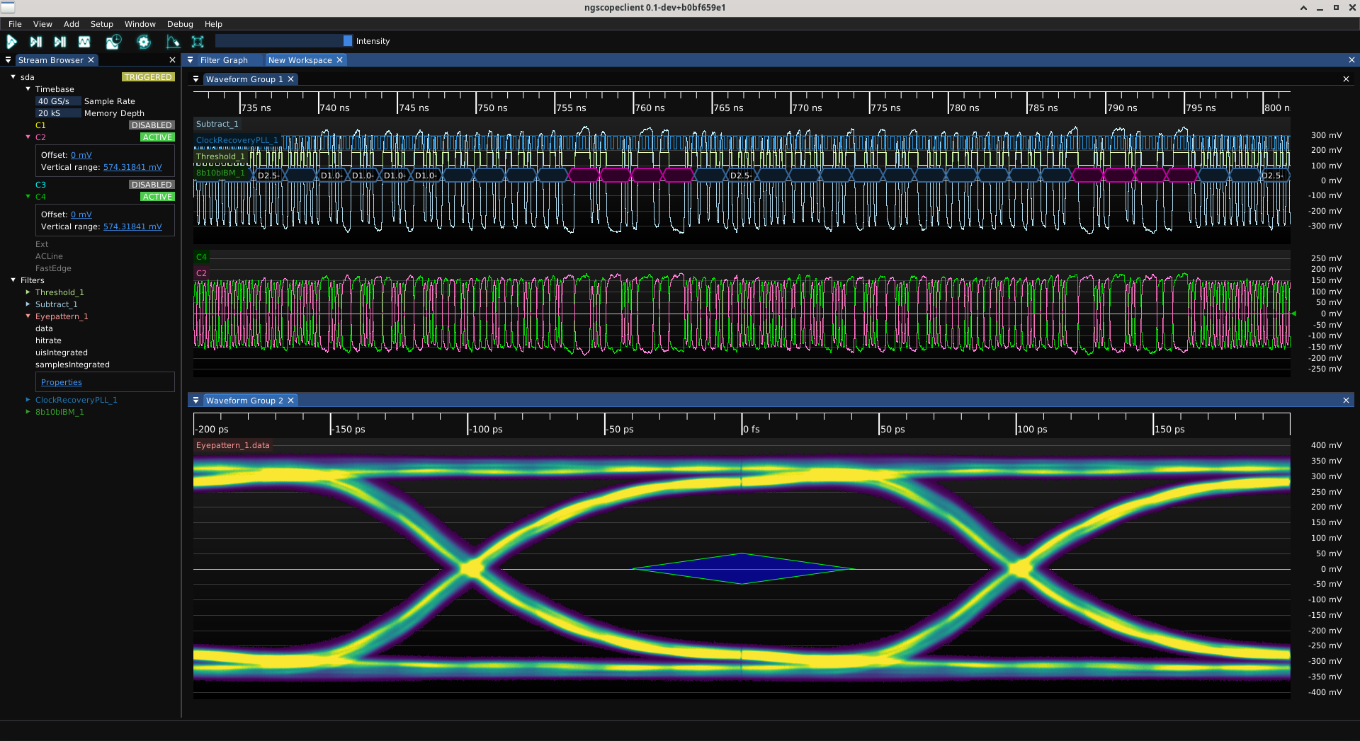
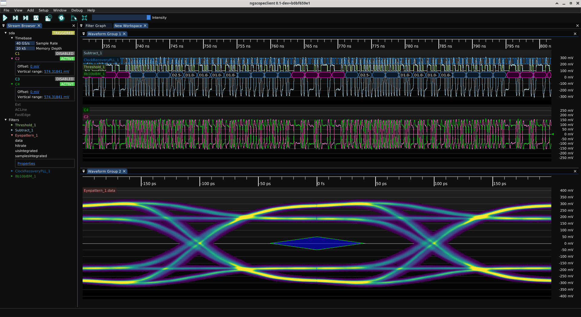
As a test I tried turning it up much higher, to 0x0f, to see if I was poking the registers right. This worked, but gave a grossly overequalized result.
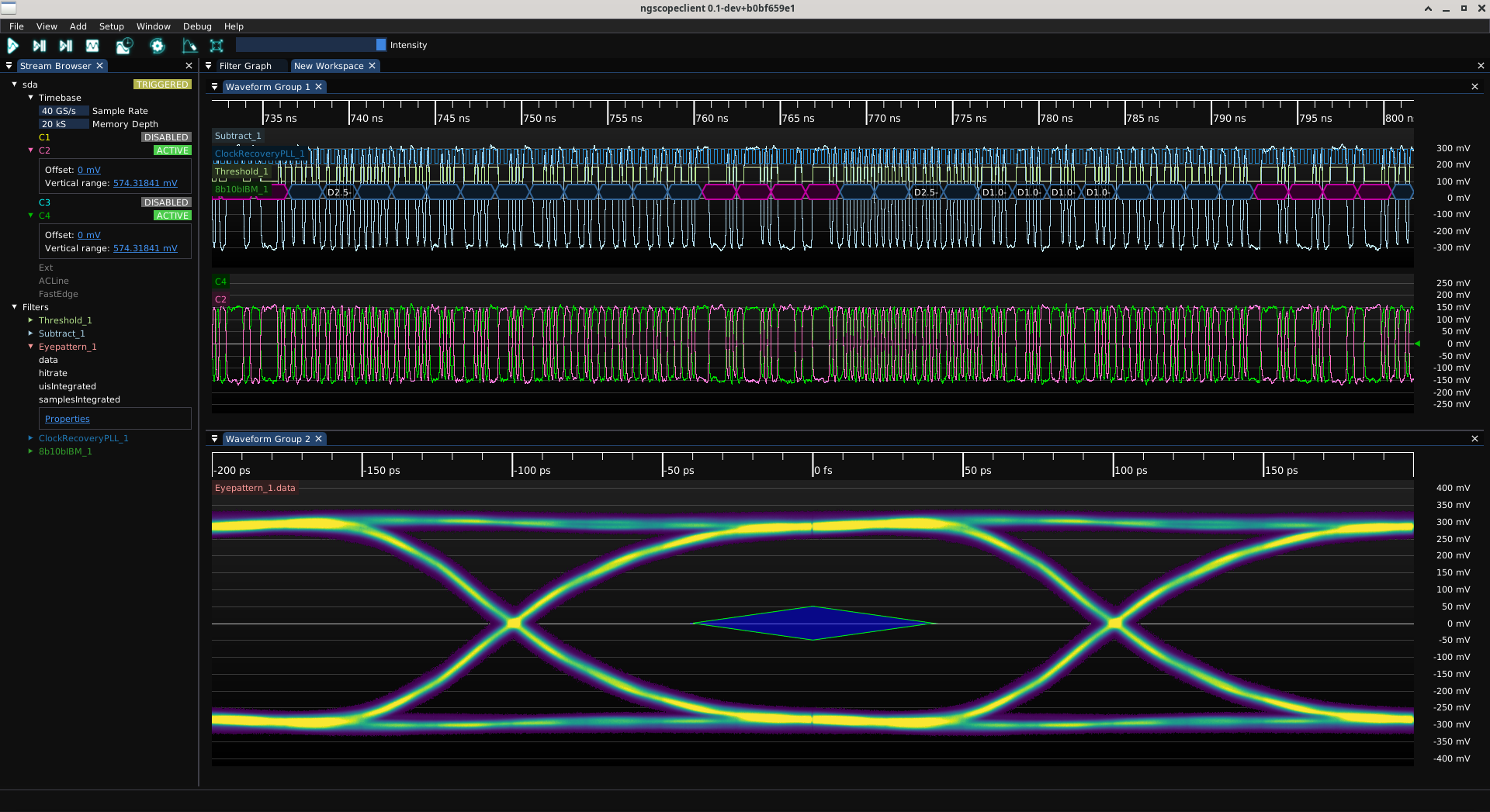
I was happy with how things looked at 0x04. The eye is fully open, all bits are the same height, and the eye is open enough to drive a bus through. This is through a foot of Samtec ARC6, two feet of Koaxis KF086, two ARF6 connector transitions, a SMPM connector launch, and about 75 mm of total PCB trace.
The eye actually passes the QSGMII transmit eye mask, not just the RX mask shown here. I think it’ll do.
Conclusions
Who needs NDAed datasheets when you can just read public driver code and work out the bits they’re not telling you?
There’s room for a lot more fun, maybe one day if I’m bored I’ll try getting code execution or a ROM dump or something out of the 8051 on the PHY. But for now the signal integrity tweaks are done so mission accomplished.
Like this post? Drop me a comment on Mastodon