Intermediate Bus Converter
(Sorry for the slow updates… I’ve been busy with a lot of stuff, like getting ngscopeclient ready for the full v0.1 release at the end of the year. I haven’t stopped working on projects, just been too busy to do long-form writeups.)
When I started out with digital electronics, most of my designs ran on 5V from a barrel jack. This was fine for simple stuff, but I rapidly ran into two problems: 5V isn’t high enough for designs that use a lot of power (at least, if you want to avoid a ton of losses in cables), and barrel jacks aren’t super reliable. They rely on just a few points of contact so it doesn’t take much of a bump of the cable to cause a momentary loss of power.
Moving to 12V was the obvious way to solve this (and I did make a few boards that took 12V on a barrel jack), but I also wanted to move away from barrel jacks. Even 12V starts to become questionable for longer range power distribution at higher power levels, so a lot of datacenter-type DC buses use even higher voltages, such as 48V.
I also wanted to use a DC bus that was non-isolated (i.e. negative supply rail is at earth ground potential) since a lot of the projects I have in mind are test equipment or rackmount networking hardware that will have grounded shields on connectors. It’s important to note that I’m using +48V here, rather than the -48V power (positive supply rail at earth potential) that is commonly used in telco applications.
After a bit of digging, I found that Mean Well makes a power brick (GST280A48-C6P) that puts out ground-referenced +48V on a locking 6-pin Molex Mini-Fit Jr connector, with up to 280W output. This is enough to run quite a few of my planned gizmos (most with <25W power budget) from a single DC bus if I made some kind of DC PDU or distribution panel.
There’s just one problem: while 48V is great for long range distribution, it’s difficult to step directly from 48V to typical digital core voltages (often <1V for modern devices). You normally need to step it down to an intermediate voltage, usually something in the neighborhood of 12V, and then go from there to whatever your actual loads require.
Enter the intermediate bus converter.
Defining the requirements
At a high level, the job of an IBC is pretty simple: take in a high voltage (48V DC in my case) and step it down to a lower voltage (12V DC). But since this was going to be a system-level power supply, I wanted this to be a bit more than just a naked buck converter, so I drew up a few initial requirements:
- 48V DC input on a 6-pin Mini-Fit Jr compatible with the previously mentioned Mean Well brick
- 12V DC output on an 8-bit Mini-Fit Jr, maybe PCIe 8-pin compatible (this ultimately didn’t happen)
- Remote on/off via a GPIO to support soft power on/off
- Soft start to avoid excessive inrush when driving loads with a lot of input capacitance
- 3.3V DC auxiliary output to power rail/reset supervisors, soft power, and other standby logic
- Temperature, voltage, and current sensors plus an I2C interface for querying them
- Some additional EMI filtering and bulk capacitance
Version 0.1
The first iteration of the IBC was 87 x 80 mm in size, targeting the OSHPark 2-layer 2oz copper stackup. Back side was almost completely solid ground with a handful of signal net crossovers, while the front side contained an S-shaped power path with monitor/control signals around it.
This design set the general stage for all of the subsequent designs, and all future versions have retained electrical (though not always mechanical) interface compatibility: 5 pin PicoBlade connector containing the 12V enable, I2C, and 3.3V standby rail. The I2C bus contained a temperature sensor at 0x90 and the management microcontroller at 0x42.
The input protection and power path was pretty straightforward: a socketed fuse at the input, common mode choke and ferrite bead to avoid radiating switching noise out the input, a current shunt and some bulk capacitors, then a TDK-Lambda i3a series buck module. No explicit reverse voltage or overvoltage protection, although something would probably blow the input fuse if it were reversed.
On the output side of the buck module, there’s a bunch more capacitace, a current shunt, a ferrite, an an On Semi NCP455620 controlled-slew load switch.
In parallel with the main power path I put a 3.3V LDO to run the management logic and some voltage dividers to monitor the 48 and 12V voltage levels, plus a pair of AD8218 current shunt amplifiers to convert the shunt readings to voltages I could feed to the MCU (a STM32L031).
Version 0.2
The v0.1 IBC had one major problem: one of the tracks from the output of the buck module to the first capacitor was an 0.125mm track that was supposed to be a marker for an eventual zone fill, but I never added the copper pour! It functioned fine once I bodged a piece of copper wire across this path.
It worked well enough from a power perspective, but gave very noisy current measurements. After a bit of digging I realized the problem: the ADC bandwidth was high enough that it was picking up switching ripple through the current shunts.
So I made version 0.2 which fixed the missing zone fill and added a low-pass filter between the current shunt amplifiers and the MCU ADC.
Version 0.3
After this fix, everything worked great except that I realized I had derped and put the 48V current shunt in a high dI/dT path causing it to pick up switching noise.
So I made version 0.3, the final iteration of the first generation IBC.
Version 0.4
The i3a module had one major problem: efficiency. It ran hot (necessitating forced air cooling even at fairly light loads), and its ~3W idle power unloaded resulted in awful efficiency at the ~10W output levels required by the trigger crossbar.
While exploring alternatives, I came across the Murata MYC0409. This is a rather unique switching DC-DC architecture in that it doesn’t use an inductor like a typical buck converter. Instead, it uses a charge pump and switches a series of capacitors around.
This has one significant downside: it produces an unregulated, ratiometric output that is a fixed integer division of the input. Essentially it consists of a series of switching transistors and four internal capacitors; they are connected in series and allowed to charge off the input supply then connected in parallel and allowed to discharge into the load.
But this isn’t a huge deal for a converter intended to primarily drive fans and other DC-DC converters, and the ~800 mW idle power consumption was a huge draw compared to the i3a.
As part of the revamp, I switched from the STM32L031 to the L431 in order to get more flash so I could support a bootloader and A/B firmware slots, enabling field updates if that ever became necessary. The 32 kB of the L031 was a little small to fit two copies of the firmware plus a bootloader.
I also took this opportunity to move version 0.4 to its own repository since it’s a common component, not part of the trigger crossbar project.
The legacy v0.1-0.3 line still lives in the trigger crossbar repo history, but I have no plans to continue development of it at this time.
Version 0.5
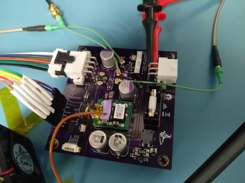
v0.4 had a few teething troubles. For starters, as soon as I applied power it exploded.
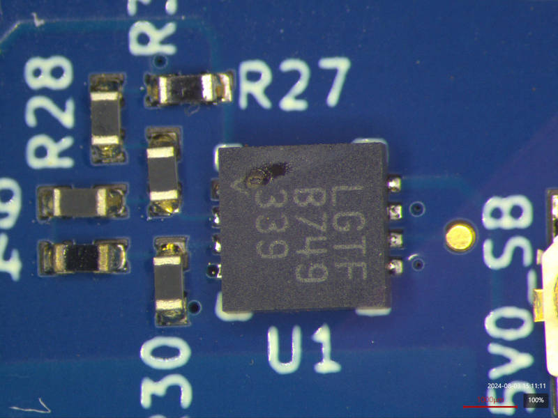
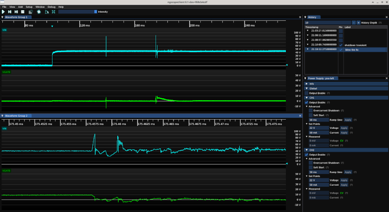
More precisely, the LTC4367 did. It looks like when power was first applied I started getting a bit of current going down the supply leads, through the input side common mode choke that I had put there to suppress potential common mode EMI, hit the LTC4367 input, then it had nowhere to go since there wasn’t much input capacitance upstream. The end result was inductive spikes peaking at close to 100V amplitude which was enough to cause the LTC4367 to pop.
I tried a few fixes without success while troubleshooting (blowing a second LTC4367 in the process), then simply removed the entire input protection subsystem to test, at which point it worked like a charm.
Weeks later, I discovered that these spikes had also damaged the 1M ohm frontend on channel 3 of that scope - presumably exceeding the V/F derating for my 10x R-C probe and overloading the input. I’ll get it repaired eventually, but the 50 ohm frontend still works fine and that’s the one I use more often so I’ll probably just red-tag the channel in the meantime.
I saved the blown LTC4367s and will try to decap them at some point and see if there’s obvious damage to the dies. If it’s not too expensive I’ll try to get one X-rayed or even CT scanned, it’ll be cool to see what happend to the pin 1 bond wire and how much carnage is inside the package.
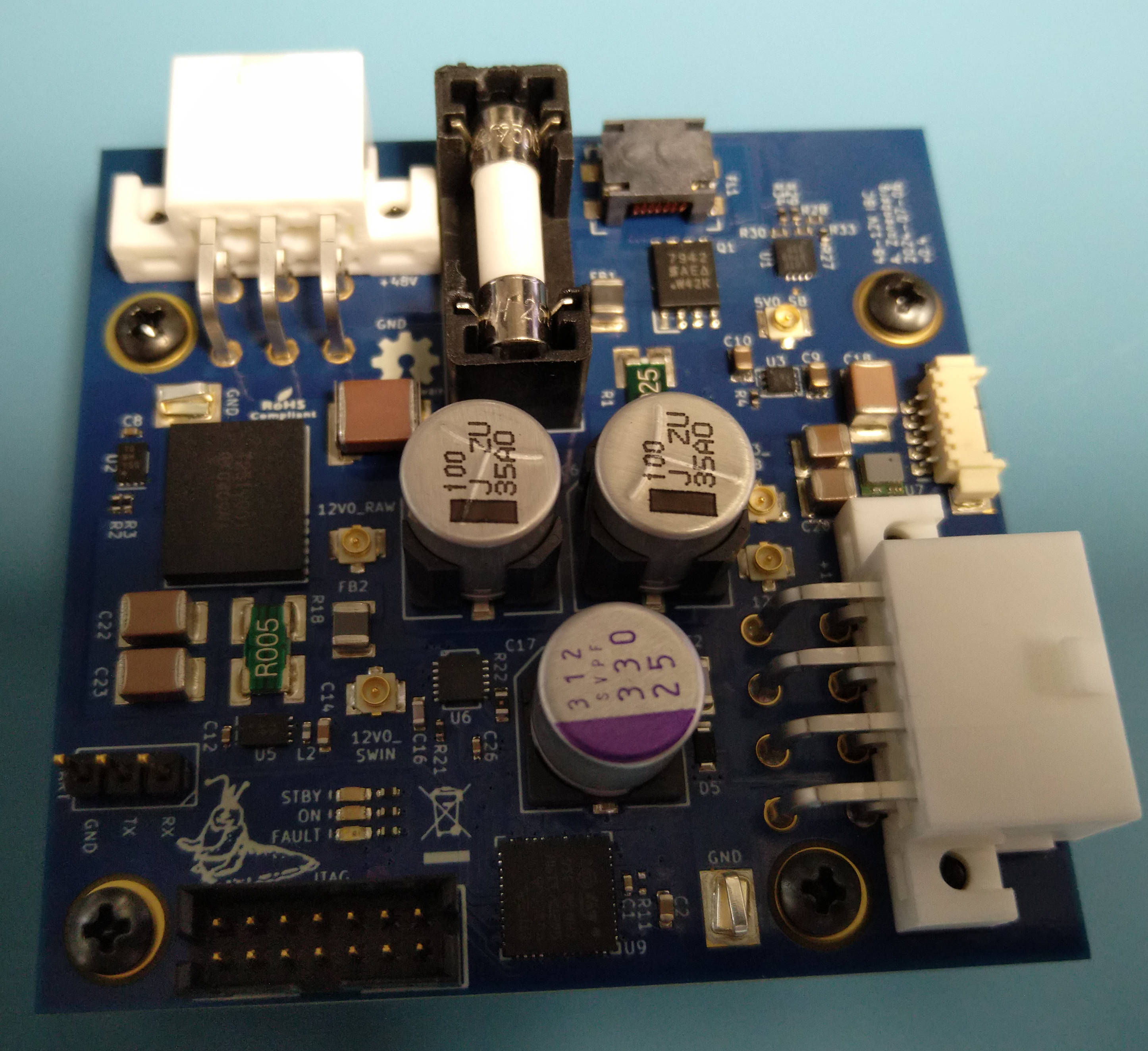
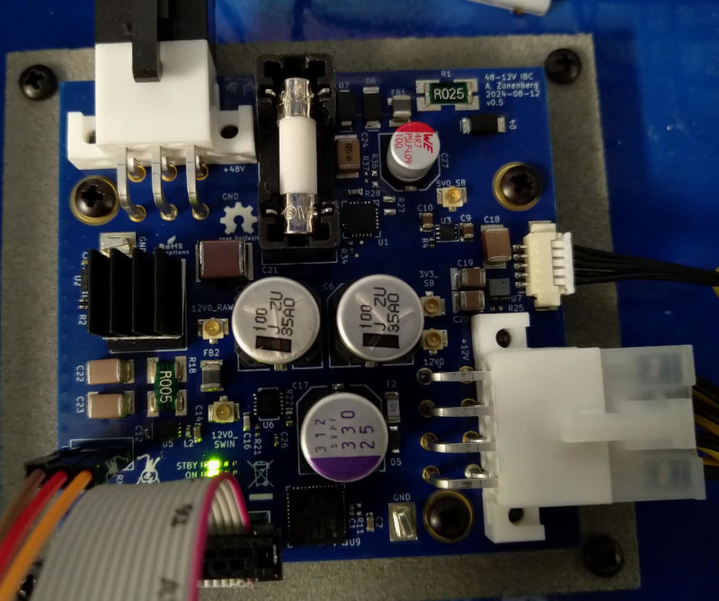
So I made one final version 0.5 which removed the CMC and LTC4367 in favor of a ferrite and TPS16630. This version also adds a few more TVS diodes and other protections against overvoltage and ESD.
This version works great and is on one of my prototype boards now, and I will probably be building a few more for testing soon.
Version 0.6 coming?
As of now, v0.5 is current. There’s one minor annoyance, the 3.3V standby rail switcher is fed by the 12V output after the ferrite bead, and could perhaps do with a small input capacitor to reduce high frequency transients. The end result is that there’s high frequency switching spikes injected into the 12V rail. Measuring with a current probe shows no corresponding spikes in current drawn by the load (unsurprising) so I don’t think this will have a huge impact on EMC and I’m just doing prototypes at this stage anyway.
My current plan is to use up all ten of the v0.5 boards I’ve built making protos of various equipment, then when I run out do a v0.6 spin with this fix and any other EMC or performance related tweaks I might want to make after having used the thing for a while in the lab.
Characterization
The only thing left to do was more extensive performance characterization.
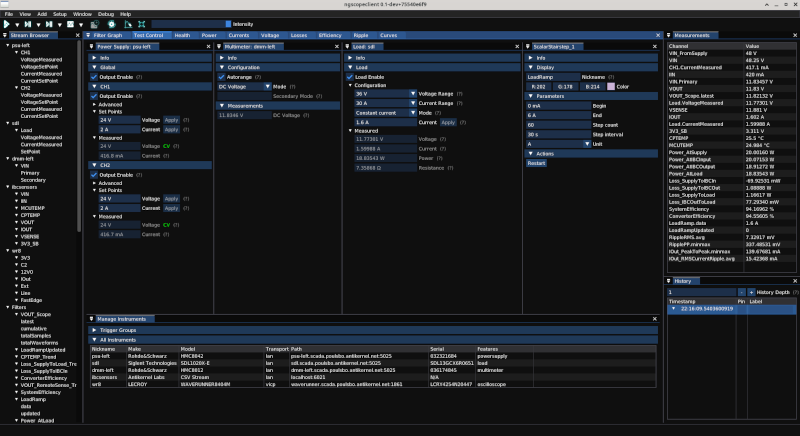
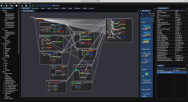
This provided a good opportunity to throw together a large filter graph to demonstrate some of the multi-instrument capabilities of ngscopeclient.
The test is fully automated, with a scalar-stairstep filter ramping load from 0 to 6A in 100 mA steps, waiting 30 seconds between steps for thermals to stabilize, and the resulting data is plotted as values vs load current.
The final characterization setup used 16 channels of data from four physical instruments (R&S power supply, Siglent load, R&S multimeter, Teledyne LeCroy oscilloscope), plus on-board sensor data streaming via SWO to ngscopeclient (I’ll probably do a more comprehensive post about this flow once I’ve fine tuned it a bit), being processed by 54 different filter graph blocks to produce the final curves.
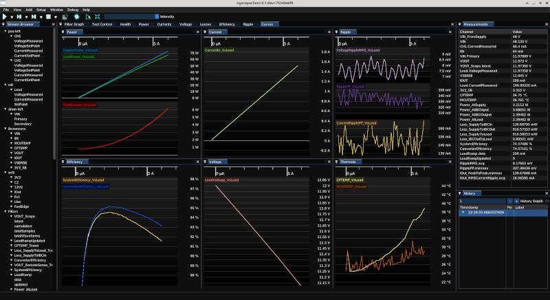
Total loss (power out minus power in) starts at about 800 mW with no load, increasing to just over 6W at max load. This is a massive improvement over the 3W idle power of the old design.
Efficiency is over 80% at very low load levels, reaching 90% at under 1A. Max efficiency (after correcting for losses in the wiring harnesses) is over 95% from 2-3A before falling to around 93% at 6A.
Output voltage does sag a fair bit at high loads, from 12V at no load down to about 11.1V at 6A. This is measured at the load and includes losses in the wiring harness, so typical chassis deployments with shorter wires would avoid a bit of this drop, but the droop is inherent to a non-regulating ratiometric converter like this (since any ESR in the output path is not being compensated by any kind of feedback network). So this isn’t something you’d want to use for a precision 12.00V rail, but as an intermediate rail that’s just feeding a bunch of buck converters it’s totally fine.
Realistically, I’m a long ways from needing 6A on any of my designs anyway. And the MYC0409 supports paralleling up to 4 modules for better performance under high load, so if I’m ever going to design something that power hungry I’d probably scale up the IBC to match.
Output ripple is only a few mV RMS, but around 330 mV p-p because of the spikes from the 3V3_SB switcher I mentioned previously.
Thermals look excellent. With no heatsink in still air the module did reach close to 100C at full load, but a small heatsink and a small amount of airflow was sufficient to keep temperatures below 40C over the entire test program.
Conclusions
I’m pretty happy with how the IBC turned out. I will eventually be doing one final board spin to fix the 3V3_SB switching spikes but I’m in no rush to do so, it’s good enough for my in-house use despite the spikes.
It’s a lot more efficient and runs cooler than the older design, has plenty of headroom for my designs to get bigger, and can scale to multiple converters if I need even more power handling capacity.
But for now, it’s going to be powering most of my large prototypes moving forward. Look forward to seeing it appearing in lots of projects coming up!
Like this post? Drop me a comment on Mastodon
