STM32L431 teardown
I realized a while back that I haven’t put any silicon reverse engineering content on the new blog yet. It’s time to change that!
Today, we’ll be doing a teardown of the ST STM32L431. Why? Because it’s a part I use a lot, it’s my go-to for “I want enough flash for A/B firmware images and a bootloader and a nontrivial amount of code, but a H735 is overkill”. And, most importantly, I had one on a scrap board in my “microscope food” bin (yes, that is the actual label on it).
Quick disclaimer before we begin (no, work didn’t make me say this): if you’re a prospective customer of my day job, be advised that all of this analysis was done for fun in my garage lab with optical microscopy and basic wet etch for deprocessing. The quality of results shown here is not representative of what I can do in a real lab with proper gear for CMP, plasma etching, SEM/FIB, etc.
Some quick stats
In total, the analysis in this post took about two days (much of that waiting for imaging, not actively doing stuff). I acquired 49.2 GB of optical imagery (90436 individual image files, including focus stacked/stitched intermediates) at a range of magnifications. All of the stitched datasets (at least the ones that turned out good) can be viewed on siliconpr0n, I’ll be linking some of the more interesting ones here. If you want to see more, definitely click around all of the delayered scans though.
Delayering was done with Whink rust remover (1-3% HF per the SDS, I really should do a titration at some point to figure out the actual concentration) followed by mechanical cleaning to remove delaminated copper interconnect and vias.
Imaging used a Labsmore LIP-X1 CNC microscope with a Mitutoyo VMU optical column. Objectives used were Mitutoyo plan apo 20x/0.42 for overviews and in-process inspection and Olympus Neo SPlan 100x/0.90 for high magnification closeups.
Device Overview
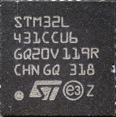
The STM32L431 comes in a bunch of different packages ranging from a 49-ball WLCSP up to 100-pin LQFP. The sample seen here came from a 48-pin QFN.
It contains a Cortex-M4 with FPU capable of clocking up to 80 MHz, 256 kB of flash memory, 64 kB of SRAM, a 12-bit ADC, dual 12 bit DACs, an opamp, two comparators, and a bunch of other goodies.
Top metal
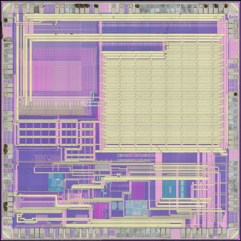
The overall die size, including scribe line, is approximately 3.132 x 3.127 mm = 9.793 mm^2.
Several features are immediately apparent:
- The device is made on a fairly modern, high layer count process (Wikipedia claims 90 nm, we’ll verify that). Power routing covers most of the surface, preventing us from getting a good view of a lot of the chip.
- A regular region in the northwest corner looks like it’s probably some kind of memory
- The south and southwest region looks analog
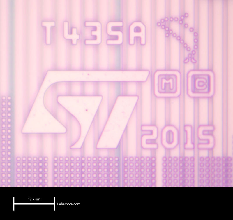
Looking at the northeast corner we can see internal part number “T435A”, a 2015 die copyright, the ST logo, and a little doodle of a dolphin. It always brings me joy to see silicon artwork, which has become less common in recent years.
This is the second dolphin I’ve seen on a recent ST chip (the STM32H735 has one too). Anybody know why? Internal project codename? Design team mascot? Local sports team at one of the offices?
EDIT: According to folks at ST, it’s actually an orca, not a dolphin. The part was codenamed “Orca” during development.
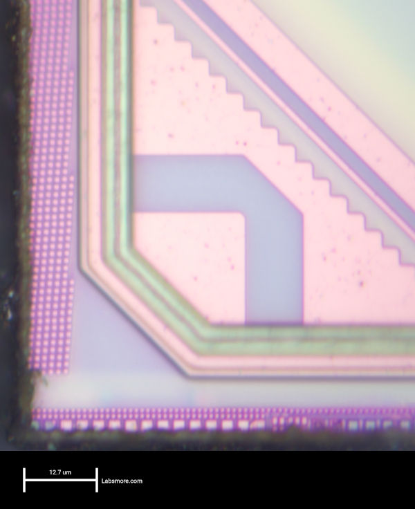
Unlike some of the other STM32s I’ve looked at, this one isn’t made in house at ST’s foundry - it’s made by TSMC. The fiducial in the corner is a dead giveaway. The overall appearance is consistent with the 90nm node but we can do some more digging to be sure.
Substrate floorplan
I deprocessed the sample to bare silicon substrate (going slowly and grabbing a lot of photos on the way, we’ll get to those in due time).
While it’s a bit tricky to tell with only wet etch deprocessing and sub-optical feature sizes, the STM32L431 appears to be seven copper and one aluminum metal layers for a total of eight metal layers.
The 20x scan of substrate with no annotations is on siliconpr0n. I took a 100x scan but had significant stitch artifacts in the memories so I didn’t upload it (but you’ll see crops of the nicer regions in this post). At some point I’m going to try to re-stitch and will add a link here if it turns out well.
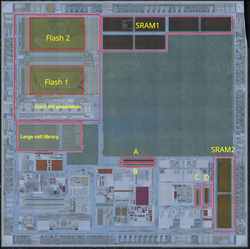
At the substrate layer, we can see the pad ring around the perimeter, analog in the south, large memories in the northwest, and standard cell logic in the northeast. Several small memories (marked A through D in the floorplan) are present along the edges of the analog region. SRAMs A and B use the same bitcell as SRAM1, while C and D use the same bitcell as SRAM2.
Three smaller regions of standard cells can be seen outside the main logic area, sandwiched between the flash memory and theanalog region. Two of them are rectangular and use a different cell library than the rest of the chip (with a much larger row height), while the third is L-shaped and uses the same cell library as the main digital region.
Memories
SRAM1
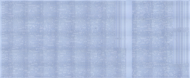
At the north end of the die is SRAM1. This is a 48 kB single-port SRAM consisting of three identical 16 kB memory IP instances.
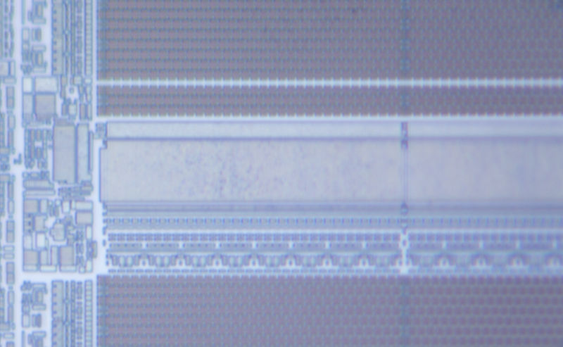
Each SRAM IP measures 796 μm x 201 μm (0.16 mm^2) and consists of two blocks of cells on either side of a central addressing spine, plus two spare columns for array repair between the central spine and the main east bitcell array.
Each block is 381 μm (256 columns at 1486 nm pitch) wide, and 179 μm (4 strings of 64 rows at 680 nm pitch) high for a total capacity of 64 Kbits (8 KB) at a density of 1.04 μm^2 per bit or 939 Kbits/mm^2 (not counting periphery). The overall array density including periphery is 1.22 μm^2 per bit or 800.5 Kbits/mm^2.
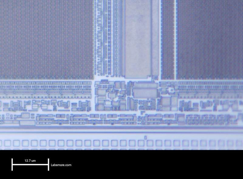
The 1486 x 680 nm (1.01 μm^2) bitcell uses a lithography-optimized (all poly running horizontal) 6T bitcell design typical of modern planar CMOS technologies.
Dummy features appear to be present around the perimeter of the array.
SRAM2
SRAM2 is a single 16 kB block in a separate power domain from the rest of the device, which can optionally be preserved across device resets and kept active in an intermediate low-power state in which SRAM1 is not preserved (in the deepest sleep states only the 128 byte backup SRAM is preserved and contents of both SRAM1 and SRAM2 are lost). It also has optional parity (error detection only, not full SEC-DED ECC as present on some higher end STM32s).
SRAM2 is 883 x 202 μm (0.18 mm^2), roughly 11% larger than SRAM1 for the same usable capacity which aligns well with the overhead of the parity bits. Each block is 426 μm x 178 μm and, as with SRAM1, there are two spare columns for error correction.
The 1482 x 676 nm (1.00 μm^2) bitcell is identical in overall size to the SRAM1 bitcell within the bounds of measurement error, but has a different appearance (most notably, a different color as seen at lower magnification). This is likely due to SRAM2 being optimized for low leakage, perhaps using HVT transistors in the bitcell (although interestingly, the datasheet makes no mention of it having worse performance: perhaps it is placed closer to critical paths in the interconnect to compensate for higher clock-to-out delay? I haven’t actually run any microbenchmarks to see if there’s a pipeline register or anything in the path).
Dummy features appear to be present around the perimeter of the array.
SRAM A (tentatively flash instruction cache)
SRAM A uses the same bitcell as SRAM1, and consists of 32 rows x 256 columns (plus two spare), for a total capacity of 8 Kbits or 1 kB. Unlike the larger SRAMs, this one only has a single tile array (with the addressing logic on the west and north sides) rather than a double array with row addressing down the centerline.
The 1 kB size and 32 x 256 array structure is consistent with the I-side flash cache (32 cache lines of 4 x 64 bits words).
SRAM B (tentatively flash data cache)
SRAM B is identical to SRAM A, but only 8 rows high. Its placement very close to SRAM A, as well as its size of 1 Kbit or 256 bytes, is consistent with the D-side flash cache (8 cache lines of 4 x 64 bits
Neither SRAM A nor SRAM B have obvious extra bits which could be used for cache line validity state or tag. The flash is 256 kB (logically 32K 64-bit words) so assuming a fully associative cache (plausible for one this small), 15 tag bits per line would be required, plus a validity bit. This would require an additional 512 bits (for I-cache) and 128 bits (for D-cache) of tag memory, likely implemented as discrete flipflops to enable parallel tag matching.
SRAM C
SRAM C uses the same low-power bitcell as SRAM2, and is 128 columns x 32 rows (4096 bits, 512 bytes) with two spare columns.
Its functionality is unknown, perhaps the RTC backup SRAM, CPU register file, or SDMMC TX/RX FIFO?
SRAM D
SRAM D uses the same low-power bitcell as SRAM2, and is 128 columns x 64 rows (8192 bits, 1K bytes) with two spare columns.
Its functionality is unknown.
Flash
The datasheet capacity for the flash is 256 kB with ECC (so a physical capacity of 288 kB), organized as 72 bits physical / 64 bits logical by 32768 words.
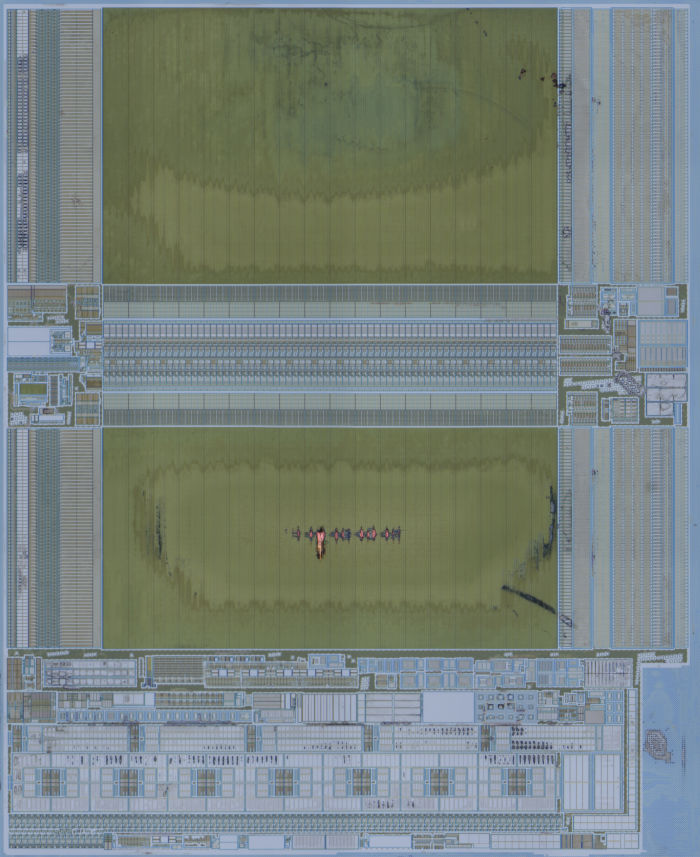
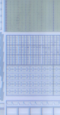
The flash memory is located in the northwest corner of the device. It consists of two blocks, one 25% longer than the other. This is consistent with 128 kB for the small half and 128 kB + 32 kB system memory (28 kB boot “ROM” and 4 kB trim/OTP region) for the large half, plus ECC.
Overall IP size is 1027 x 965 μm for the main memory array (0.99 mm^2) plus 955 x 300 μm (0.29 mm^2) for the high voltage generation block.
The lower bitcell array (128 kB logical, 144 kB / 1152 Kbit physical) measures 684 x 334 μm (0.23 mm^2). This gives a density of 0.194 μm^2 per bit or 5034 Kbits/mm^2 - 5.36x higher areal density than the 6T SRAM bitcell.
The overall flash structure is 18 copies of a “super-column” tile, subdivided into four copies of the basic column circuit, giving a total width of 72 columns (as expected from the datasheet).
The visible wordline structures have a pitch of 1.28 μm, and the entire array appears to be 260 wordlines high (likely 256 + dummy features)
Each column appears to have 4-way muxing, giving a physical array width of 288 bits. Bitline logic within each column has a pitch of 2.24 μm, while column logic has a pitch of 9.50 μm. This gives a tile size of 1.28 x 2.24 = 2.86 μm^2.
The 288 x 256 cell array which can be inferred from this image analysis, however, only gives a capacity of 72K tiles - 16 times lower less than the known 1152 bit physical array capacity. This suggests that the actual bitcell structure is significantly smaller than what we can see here.
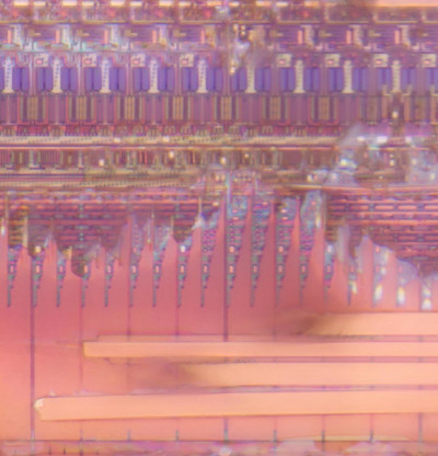
Backing up to the intermediate deprocessed stages, we can see some more details: the column mux logic on metal… 2, I think, contains a diagonal structure which appears to consist of 8 wires at roughly 466 nm pitch, fanning out to unseen logic further down the stack. This suggests a 466 nm bitline pitch and a physical array width of 1152 bits, not 288.
This still requires additional row logic: 1152 Kbits with 1152 bitline array width would require a 1024 wordline height, not the 256 tiles visible here. There appears to be a 4-way symmetry in the wordline logic as well, which is consistent with this.
This suggests that the actual wordline pitch must be closer to 320 nm (and the green horizontal structures seen here are not wordlines, but strings of bit cells too small to resolve optically), giving an approximate bitcell size of 320 nm x 466 nm or 0.15 μm^2, consistent with the overall array density of one bit per 0.194 μm^2.
Main logic area
The digital core of the device measures 1.652 x 1.54 mm, with a small cutout (824 x 226 μm) in the northwest corner for SRAM1. This gives an overall logic area of 2.36 mm^2. At a 100% packing density of 413K gates/mm^2 from literature for an unspecified TSMC 90nm cell library this gives an upper bound of 974K gates; actual packing density will be lower (maybe around 750K NAND2 equivalents).
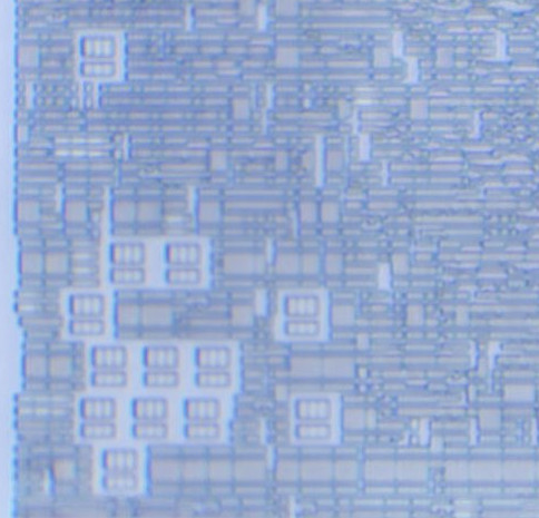
The library height is approximately 1.95 μm.
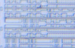
At metal 1, we can barely resolve the ~300nm wide power tracks and almost no details within the cells are visible.
Low density logic area
A small region at the center west part of the die, approximately 792 x 323 μm (0.26 mm^2), uses a different cell library with a much larger height (approximately 3.42 μm). Without much in the way of supporting evidence, I suspect this is the backup domain logic with the RTC, backup registers, tamper logic, etc, using an extra low leakage cell library.
At metal 1, we can make out substantially more detail in the cells than with the high density library used elsewhere in the device.
Conclusions
I’m not going to do a full netlist extraction or anything, this is just a high level teardown. It focuses on memories and logic because those are the portions I’m most familiar with - if anybody knows their way around PLLs, ADCs, DACs, etc. and wants to do some analysis on the mixed signal stuff I’ll gladly throw raw data your way.
There wasn’t really any specific goal to this analysis, just spending some time getting extra familiar with a part I use all the time. Hope you enjoyed!
Like this post? Drop me a comment on Mastodon
