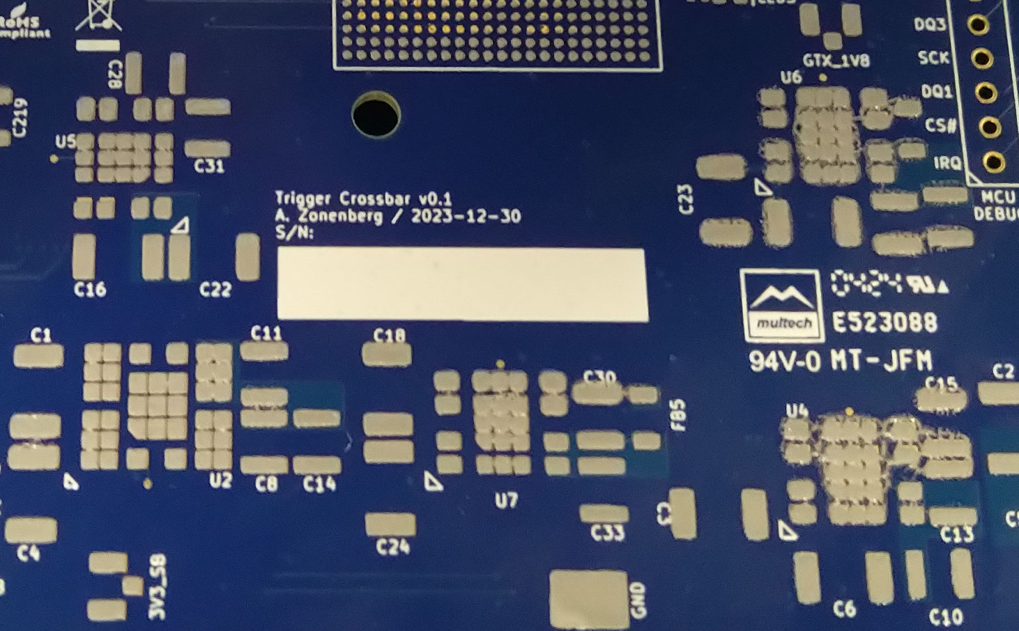
Trigger crossbar
If you have a large, well-equipped electronics lab you’re going to have a lot of instrumentation with trigger input and output ports.
In my case all three oscilloscopes, the vector signal generator, and even my VNAs have trigger sync capability, and there’s probably more things I’m missing. And that doesn’t even count the ThunderScope or the two Siglent AWGs I have on loan for ThunderScope R&D.
Very often, it’s handy to cascade these in order to enable complex multi-instrument setups (for example, having a scope trigger when an AWG creates a pulse of some sort, without burning a scope channel to look at the AWG output, or to have two scopes trigger simultaneously to capture more channels of data in a complex system).
There’s just one obvious problem: All of my equipment is rack mounted, there’s a LOT of it, and there’s already a ton of cable spaghetti in a fairly confined space. The last thing I want to be doing is reaching around behind the racks and crawling under the bench to untangle coax and route trigger signals from one instrument to another every time I want to set up a multi-instrument experiment.
The second, slightly less obvious, problem is that not all of these signals are compatible voltage levels. For example, the trigger output on my Teledyne LeCroy oscilloscopes is 1V into high-Z or 500 mV into a 50Ω load. The Siglent vector signal generator has a 5V TTL trigger input. So you can’t just directly connect these without a level shifter or buffer.
What if there was a better way?
The concept
Pretty quickly I came up with a high level concept for what I wanted to build: a 1U device with an Ethernet SCPI interface plus a ton of coaxial trigger inputs and outputs, connected to a buffered FPGA-based switch fabric.
Some outputs would be buffered by external level shifters to enable interfacing with different voltage levels, while others would be directly connected to FPGA GPIOs for the lowest possible jitter but with a fixed voltage range. Inputs would be routed to comparators to allow arbitrary switching thresholds.
A handful of these channels would be bidirectional, with latching relays to swap between input and output modes. This is important because a few of my instruments, most notably the PicoScope and Siglent vector signal generator, use the same BNC as both trigger input and output.
The whole thing would be powered by 48V DC using my existing intermediate bus converter and controlled over IP via ngscopeclient, using the filter graph to create virtual connections between crossbar ports..
High level design
I selected the Xilinx XC7K70T-2FBG484C as the FPGA for a few reasons:
- I had a lot of 7 series parts in inventory, so no need to buy anything new.
- Kintex-7 has high-performance (HP) I/O banks which have faster slew and lower jitter than the high-range (HR) I/Os found in Spartan/Artix parts. I didn’t want to increase cross-trigger jitter more than necessary so this was important.
- The 70T in FBG484 is the lowest cost part in the Kintex-7 line, we don’t need a ton of stuff in the FPGA so no reason to go bigger.
- The -2 speed has 10.3125 Gbps capable SERDES (we’ll get to why this is important in a bit).
This then got paired with the STM32H735 MCU as the controller.
I started this project all the way back in October 2023, long before I realized how cursed the OCTOSPI on the H735 was. In fact, many of the things I discuss in that post were learned on the crossbar project, it just took me this long to get to the point of having time to write about the crossbar as a whole.
So (foreshadowing a bit), I made the mistake of connecting it via the OCTOSPI thinking that I wouldn’t need the bandwidth of the FMC to control a few muxes and it would save pins. I also hadn’t tried the FMC yet and thought (famous last words) that the OCTOSPI would be simpler and easier to set up. This ultimately turned out to be a massive annoyance and cost me a lot of time, but I did get it working in the end.
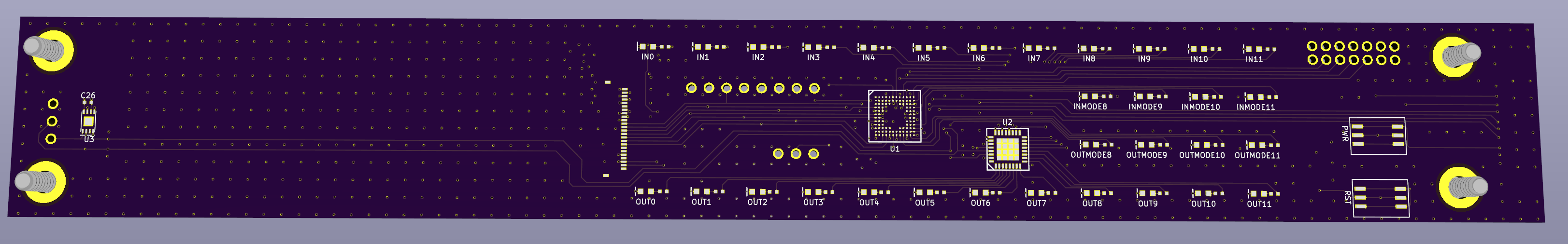
The final concept I came up with was logically a 12x12 crossbar: eight inputs, eight outputs, and four bidirectional ports.
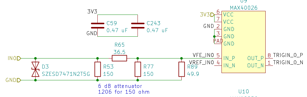
The input ports were all 50Ω impedance, with a 6 dB (2:1) attenuator and ESD diode prior to the input termination. The input then entered a MAX40026 high-speed LVDS comparator, with the positive input fed by the trigger signal and the negative by a reference voltage generated by a DAC. This design provides runtime-variable thresholding and 5V tolerance while operating from a 3.3V supply.
Output channels 0-3 were driven directly by HP I/Os on the FPGA, providing a fixed 1.8V swing but the highest possible jitter performance. The remaining 8 outputs were driven by TI 74LVC1T45 level shifters. Each level shifter had its own independent VCCIO power domain supplied by an ISL24021 power op-amp buffering a reference voltage generated by one output from an 8-channel DAC, allowing runtime adjustment of VCCIO for each port. The buffered output then passes a final ESD diode before reaching the connector.
You can see the whole schematic (and firmware) on my GitHub.
The rest of the logic board was fairly straightforward: a KSZ9031 gigabit Ethernet PHY for management (routed to the FPGA in case I wanted to add any kind of hardware offload), a bunch of Murata DC-DC modules to generate all of the necessary supply rails from the 12V intermediate bus, a serial port for initial IP configuration and debug, an EEPROM to store the MAC address, and a connector supplying power and SPI to the front panel board.
The FPGA has four GTX SERDES lanes in a single quad. I hooked them all up (it always seems like a shame to not pin out transceivers to something):
- Two lanes to front panel TX/RX differential SMA ports for use as a 2-lane BERT or serial pattern generator/receiver. I’ve wanted to build a proper BERT for a while and this was a good opportunity to play with it.
- One lane to a back panel 10G SFP+ (because why not, 10GbE is always handy to have)
- One lane TX to a front panel differential SMA port for use as a deskew reference
- The RX of the split channel went to a comparator and single-ended coaxial input for a potential future CDR trigger feature.
Unfortunately, having all of the transceivers in a single quad was a bit limiting due to the 7 series clocking architecture: they share the same QPLL, which has to be at 10.3125 Gbps for 10Gbase-R operation. While the CPLLs can be configured freely, they have a lower Fmax which meant that the BERT / CDR trigger channels cannot operate at arbitrary frequencies above 6 Gbps (most notably, 8 Gbps operation for PCIe gen3 mode is not available).
In theory it would be possible to reconfigure the QPLL for PCIe gen3 at the cost of temporarily disabling the SFP+ but current firmware/gateware doesn’t support this. Using an UltraScale+ FPGA (which has a much higher CPLL frequency range, plus two QPLLs per quad) would also have provided a lot more clocking flexibility, but would also increase the cost since I didn’t have a suitable FPGA on the shelf at the time and this board started out as a “junk box build” from parts I mostly had on the shelf already.
The PCB
The board was fabricated at Multech on the 10-layer stackup I’ve used for my last few high-end designs: SGS GPPG SGS, with TU872SLK between the signal and reference layers and S1000-2M between the power and ground layers since there’s no reason to use an expensive low-loss laminate on a power layer.
All of the trigger I/Os were placed in the northwest corner, with what ultimately turned out to be perhaps a bit too much packing density in retropect. The other rear-panel connectors were RJ45s for RS232 (Cisco pinout) and 1000baseT and the SFP+ for high speed I/O.
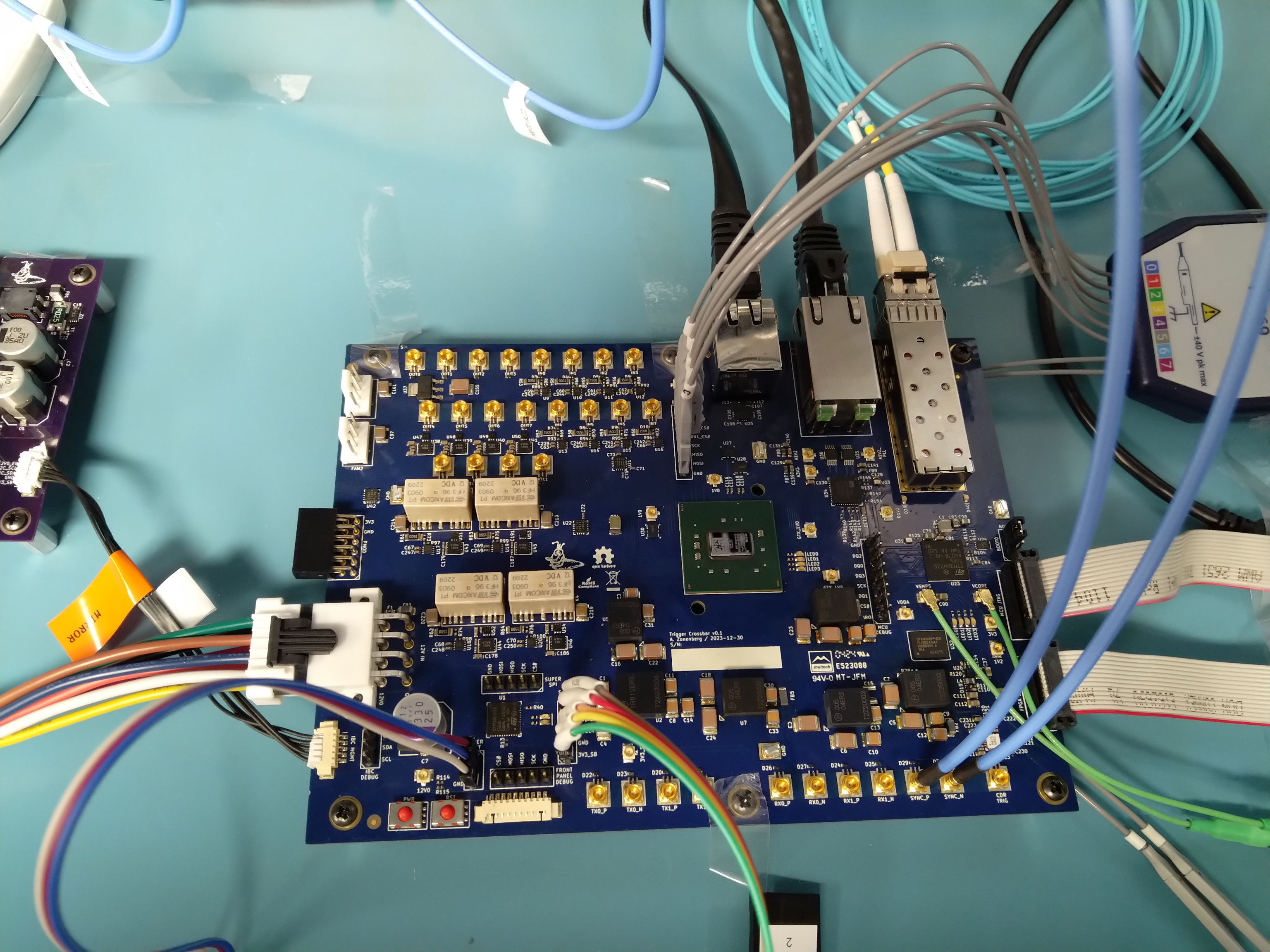
The 12V power input and I2C interface to the IBC were placed in the southwest corner, with the front panel SERDES ports along the south edge and the FPGA roughly centered in the board for easy access to everything. All of the high speed I/Os used SMPM connectors, my go-to for high speed high density these days because they’re much smaller than SMA and have higher bandwidth. But this many of them was perhaps a bit excessive; if I were doing it again I’d likely have used some kind of multi-lane board to board or board-to-cable connector and then broken out elsewhere.
The MCU was jammed into the 3 o’clock position just south of the SFP+; since it was mostly a “brain on a stick” hanging off the quad SPI link to the FPGA and not needing much IO of its own it could be placed almost anywhere.
I also provided a PMOD for debug GPIO, a couple of LEDs, and two 12V 4-pin fan connectors (only one of which ended up being used).
The final board size was 165 x 121 mm with 633 components, one of my larger designs to date. Mounting holes were 4-40, 5mm in from each corner plus one in the center of each of the long edges.
Bringup woes
Once I assembled the board (most of a weekend worth of tweezering components) and started trying to write firmware and gateware, I ran into problems. Well, actually I found one even before finishing populating the board (the SFP+ was recessed too far, and the EMI fingers on the bottom were bumping into the PCB surface and tilting it up slightly). I was able to fix this by cutting the EMI fingers off.
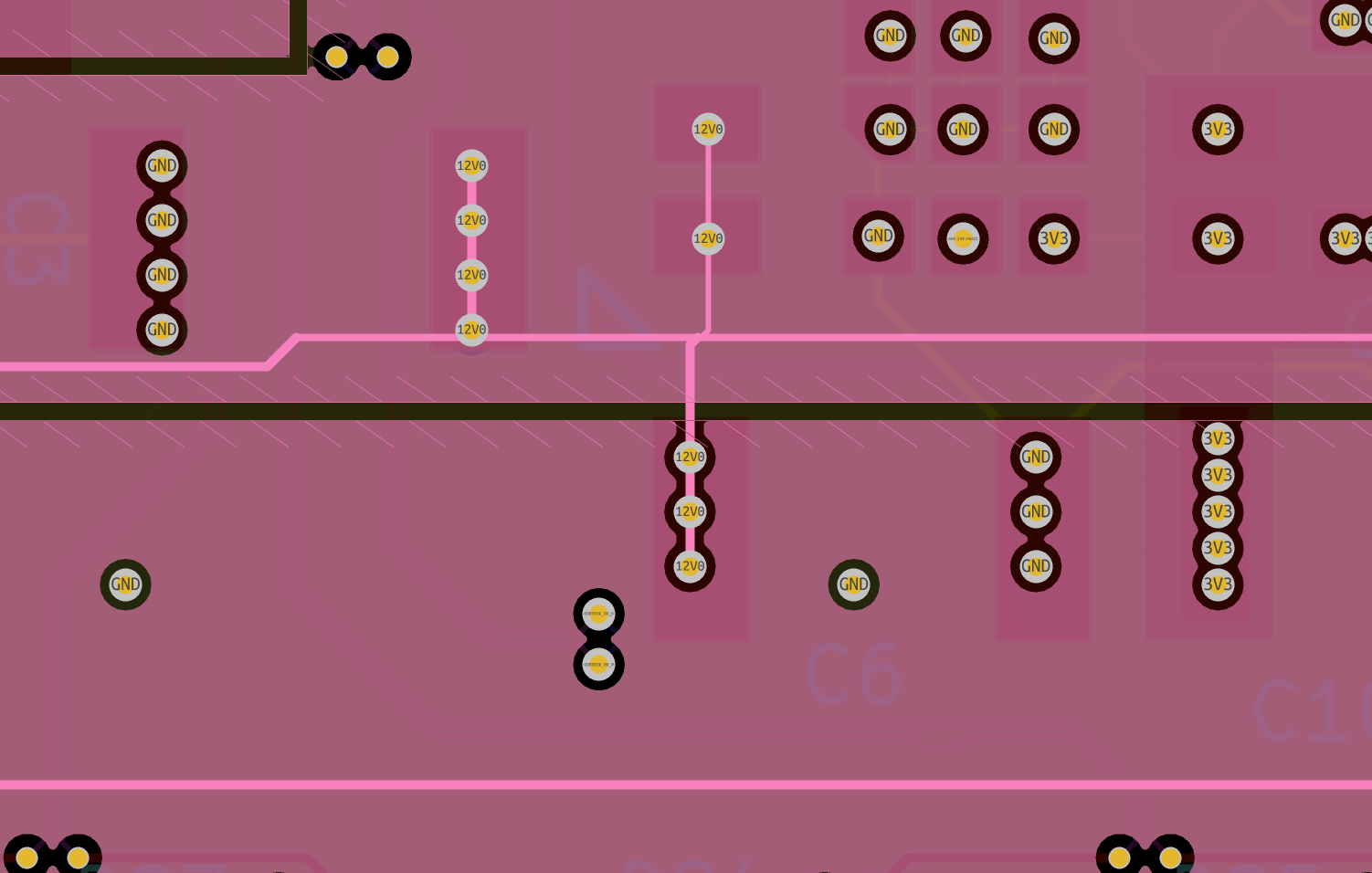
Power connection
Then I tried to actually turn it on, and nothing happened. The 48V IBC connects to the logic board via two connections - an 8-pin Molex Mini-Fit Jr carrying 12V power and ground, and a 5-pin Molex PicoBlade carrying a 3.3V standby power rail, an I2C management bus, and an enable line for the main 12V rail.
After a bit of probing, I discovered that I had wired the connector as if it were 1:1 pinout (i.e. pin 1 of IBC connector to pin 1 of logic board connector). But standard PicoBlade cables are wired straight through (a strip of parallel wires with one connector on each end, pin 1 wired to pin N-1).
I briefly considered reworking the IBC or logic board before realizing that bodging the cable was a much simpler solution. All I had to do was gently push in the latching pin on each crimp terminal to remove it from the plastic housing, then reinsert them in the correct order and add a bright orange stick-on warning label “mirrored pinout” so I didn’t mix up this special cable with a standard-pinout one.
With that fixed, I was at least able to get power to the board. There was no magic smoke, always a good sign.
More power issues
I normally have the majority of power rails on my boards default to the off state, then turn them on one at a time under control of a supervisor MCU which functions as a PMIC (in this case a STM32L031). This is great for prototypes and small-run boards because it lets me change rail sequencing dynamically with a software patch, as well as automating bringup one rail at a time with instant panic-shutdown within milliseconds if a rail doesn’t stabilize when and where it should. This minimizes the chance of hardware damage in case of solder defects or PCB design bugs on a hand soldered prototype.
Right out of the gate, things weren’t too happy: 1V8 was reporting no-good on PGOOD. 3V0_N and GTX_1V8 weren’t coming up, GTX_1V0 was unstable, and 1V2 was a dead short to ground.
Scoping the 1.8V rail gave a somewhat surprising result: the rail came up fine, stabilized at 1.7903V, but PGOOD never went high and after a few ms the supervisor assumed the rail was shorted (it wasn’t monitoring the actual rail voltage with an ADC, just PGOOD reported by the regulator) and entered panic-shutdown mode to protect the board.
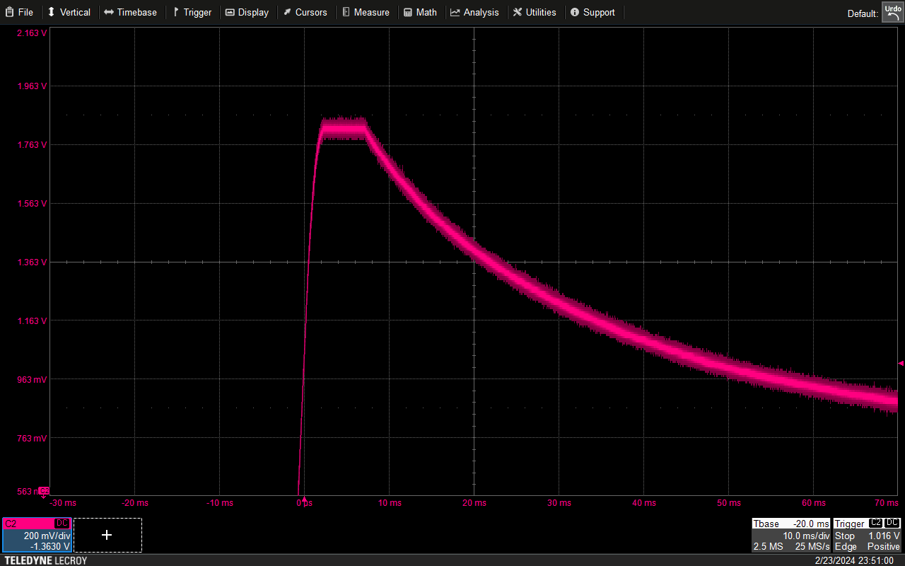
I decided to ignore the PGOOD fault since it looked like it would be a pain to rework due to the thermal mass of the board, and just patch the supervisor firmware to continue bringing up other rails a fixed delay after turning on 1V8. This isn’t something I would do in a “real” system of course, but for a one-off it was a risk I was willing to take after having confirmed the rail wasn’t in fact shorted (I had plenty of other fusing and protection mechanisms, the software timeouts were deliberately paranoid for bringup).
Most of the other rail issues turned out to be bad solder joints on the LGA Murata DC-DC modules I was using… my solder paste print in this area was decidedly subpar (the board was larger than I was used to and flexed in the printing fixture due to insufficient back-side support while only fixturing it from the edges). In retrospect I should have just wiped the board off and re-printed but I had faith in my solder paste. A bit too much faith.
Anyway, I pulled and resoldered the 1V2 and GTX_1V8 DC-DC Modules, and added more capacitance to the 3V0_N regulator input which was causing instability during startup. I had ferrites on the output of GTX_1V0 and a few other rails as secondary filters but these were hurting stability so I removed them and replaced them with 0R’s.
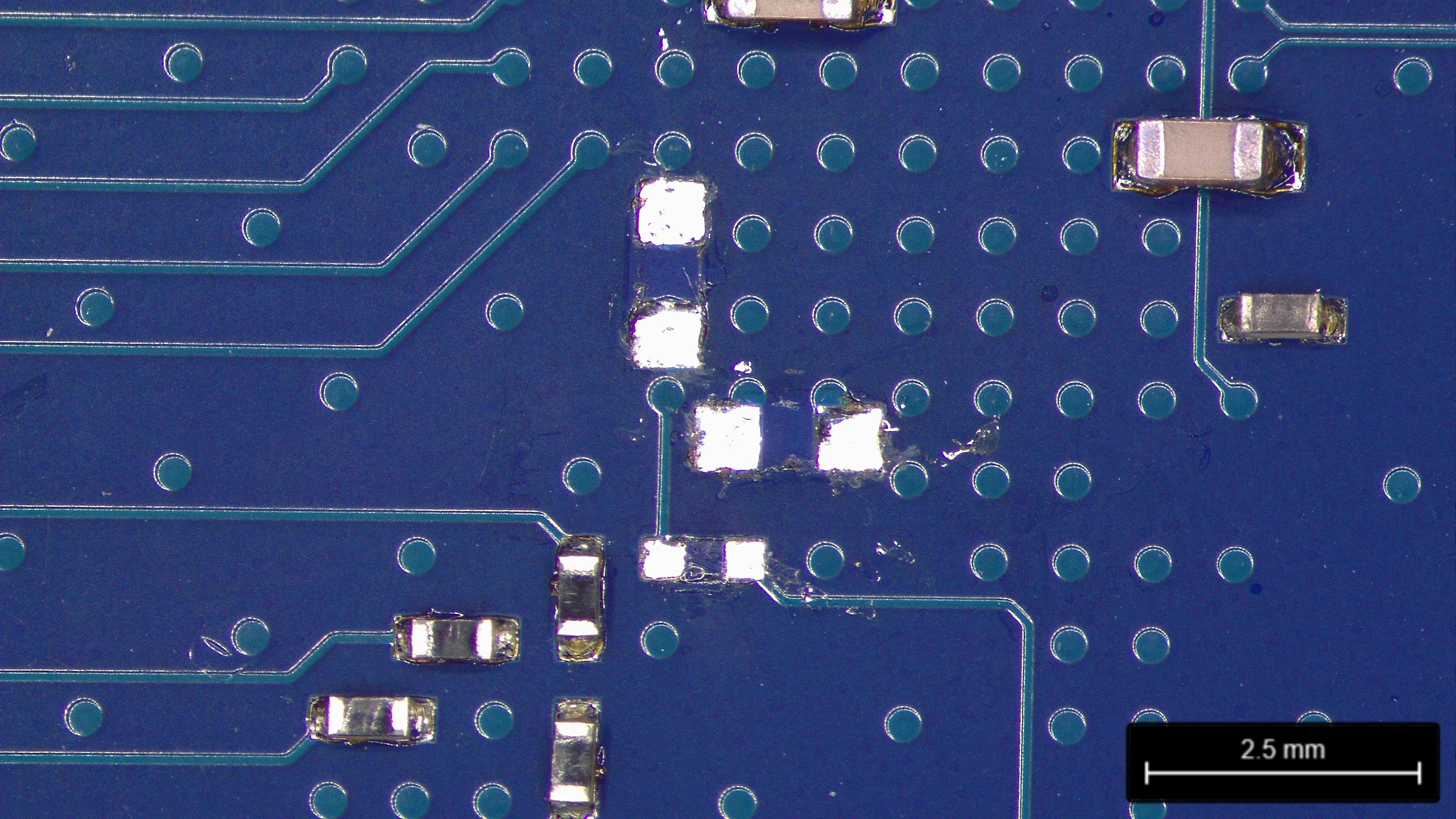
At some point I noticed that decoupling capacitor C6, one of two 22 uF MLCCs as the input of the 3.3V DC-DC module, was not actually placed within the 12V power zone fill on layer 6. The 12V terminal on the capacitor was only connected by a very thin trace coming off the vias, which significantly reduced its effectiveness. This was easily bodged with a surface jumper connecting it to C3, the other 22 uF capacitor.
Comparator Vcm issues
With the power reasonably stable, the next step was to actually hook up some signal sources and bring up the I/O buffers.
They worked fine with large-swing inputs like 3.3V, but when I tried to use low-amplitude signals the LVDS outputs of the comparators weren’t toggling.
After a while, I realized that I had missed the 1.5V minimum Vcm spec on the MAX40026 comparators when designing the input stage. And since I had a 2x attenuator on the input to provide 5V tolerance, this really came out to 3V at the input. Experimentally, if the DAC for setting the comparator threshold was set below about 800 mV, I stopped getting useful results out of the comparator. This was a major problem, since these inputs were key to the functionality of the device and my LeCroy scopes had 1V full-scale output on the trigger sync ports.
A switchable attenuator is the “right” solution here - with the 2x switched in it would perform well for ~3V to 5V inputs, and with no attenuation it would accept inputs from 3.3V down to ~1V logic levels. But retrofitting eight SPDT relays and drive circuitry around the attenuators, plus figuring out how to power and control them, seemed a bit beyond the scope of reasonable rework. I didn’t want to respin the board and since this was mostly a project to scratch my own itch and not something I planned to mass produce, I wanted to avoid scrapping the board (now worth well over $2K between PCB and components, plus several days of hand assembly time).
After giving it some thought I decided that since I planned to have any given trigger input permanently connected to a specific instrument for the lifetime of the device, I didn’t actually need a runtime-switchable attenuator. So I reworked most of the inputs to have a 0 dB passthrough instead of the original 6 dB attenuator (limiting them to 3.3V input levels), keeping attenuators only on the inputs that I planned to connect to instruments which had 5V trigger outputs. This seemed to work fine.
SPI/QSPI bus issues
As I started writing firmware, I couldn’t get the main MCU (STM32H735) to talk to the supervisor (STM32L031) over their shared SPI bus. I pretty quickly discovered that this was due to a MOSI/MISO crossover that shouldn’t have been there (STM32 SPI block wants them connected 1:1, changing pin directions based on host/device mode rather than having fixed in/out pins). This was easily reworked with a few trace cuts and a surface jumper right next to the MCU.
Around this time I also discovered how cursed the OCTOSPI was. I have a whole post about this so I won’t repeat all of the details here.
Finally, I started trying to bring up the front panel MCU and lost connectivity to the debugger as soon as I tried to send SPI traffic to it. This puzzled me to no end until I realized I was being hit by STM32L431 errata 2.2.6. Basically, the pin muxing logic is broken and if you try to use PB4 as anything but NJTRST, it doesn’t actually disconnect the signal from the JTAG TAP and any logic low on the pin will reset the TAP.
I ended up working around this issue in two different ways:
- First: Patch the firmware to keep PB4 alt mode as JTRST unless actively sending SPI data back to the main processor (which will cause a momentary debugger disconnection, but allow the debugger to reconnect as soon as the SPI burst ends).
- Second: Switch from debugging over JTAG to SWD, which bypasses the issue entirely. This also frees up the JTDO/SWO pin for use as serial trace output, which I wasn’t using at the time but have since began to take advantage of.
Single ended CDR trigger input not working
I never solved this one. There was a HMC675 comparator feeding a GTX lane that I had intended to use as a CDR trigger input, but I wasn’t getting toggles on the LVDS/CML output no matter what I did. I had so many other issues on the board and the CDR trigger was mostly a stretch goal, so I just shelved it. Could be anything from a soldering issue to a bad pinout to something borked in the power supply / circuit design.
I can always add CDR trigger input functionality in gateware via the BERT lanes, it will just require a 100 ohm differential input (or terminating one of the inputs to provide a single ended input?) rather than using the 50 ohm single ended input I had originally planned.
FPGA flash pinout bug
At this point, I had all of the major issues fixed (so I thought) and I started writing firmware and gateware. I had things working pretty well, until I tried to burn a bitstream to FPGA flash so I could boot the board from a cold state without having to JTAG it.
And nothing happened.
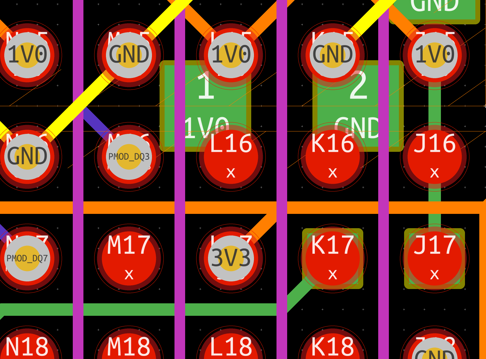
So I dug deeper, and was very upset with what I found: I had hooked CS# of the QSPI flash to CSO_B (daisy chain configuration chip select output), not FCS_B (flash chip select). I’m still not sure how I made this mistake and didn’t catch it during design review: if this was my first 7 series FPGA design it would be somewhat understandable, but it’s not. I’ve done probably 10+ 7 series designs in the past, and always got this connection right. Until now.
The actual FLASH_CS_N signal connected to pin M22 of the FBG484 package, while it should have gone to L16.
Disconnecting it from M22 was trivial, there was a via in the M22 BGA land (at the outer perimeter of the BGA) going straight into a 33Ω series terminator footprint on the back side of the board. Desoldering the terminator trivially disconnected the incorrect connection.
Adding the new connection at L16? Less trivial. In this area, there were:
- JTAG TMS and TCK in the routing channels immediately east/west of the L16 land on layer 3
- Ground planes on layers 2, 4, 7, and 9
- 3.3V VCCO power plane on layer 5, connecting to a via in L17 immediately south of the L16 land
- 1.0V VCCINT power plane on layer 5, connecting to a via in L15 immediately north of the L16 land
- 1.8V VCCO/VCCAUX power plane on layer 6, but with no vias in the immediate area
- 4.7 μF 0603 decoupling capacitor on layer 10 partially overlapping the L16 land
- The remote sense line for VCCINT on layer 10
- And of course the FPGA already soldered to layer 1
Given how far into the BGA footprint the missing connection was, trying to reach in from the edge wasn’t viable.
This really left only three options:
- Give up. Accept that SPI boot isn’t going to be available, then bodge up some board with a little MCU that acts as a JTAG controller, hooks up to the FPGA JTAG, and squirts a bitstream into the FPGA on powerup. This would require no hardware modification at all (although I’d have to design the MCU board) but would block FPGA JTAG access for debug and just be ugly. The lack of debug access alone was enough of a reason to reject this,
- Remove the FPGA, drill out a via from the top, figure out how to plate/fill it so it wouldn’t suck the solder down, reball the FPGA, put it back. I don’t have great gear for BGA desoldering, had a bunch of heat sensitive non-reflowable components on the board at this point, and didn’t feel like tweezering 484 solder balls or scrapping a several hundred dollar FPGA. So this was a non-starter as well.
- Root canal approach: add the via from the back side. This really seemed like the only way forward.
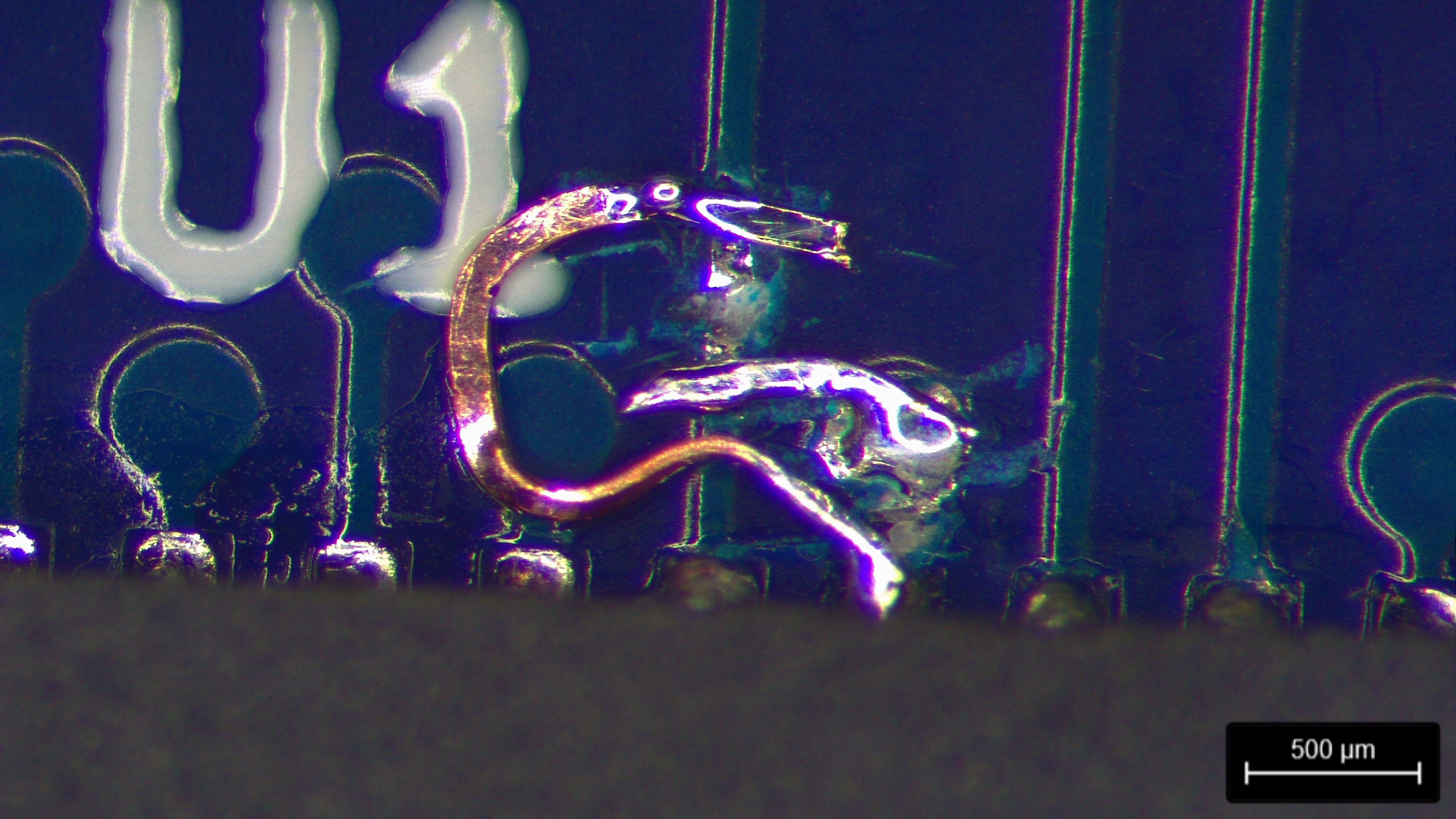
So basically I had to drill a ~1.6mm deep flat-bottomed hole, exposing but not perforating the 35 μm thick copper foil on L1 attached to the BGA land, and solder a jumper wire to it without shorting to any of the six power/ground plane layers in close proximity, damaging the VCCINT/VCCO vias 1mm centered north/south of the target, or cutting either of the layer 3 JTAG lines centered 500 μm east/west of the target. No big deal /s.
I started out by removing two capacitors and a resistor in close proximity to the work area, that were getting in the way.
Then I fixtured the board on my Sherline 5400 mini mill and loaded up a 250 μm carbide endmill. The mill is set up with a cheap Amscope stereo microscope (I’m not going to risk my nice Leica getting hit by flying debris etc) and a 1/8” collet for mounting fine-pitch drills and endmills. At the time of this project I didn’t have a proper gooseneck LED illuminator so I just used a random headlamp, although I’ve since fixed that.
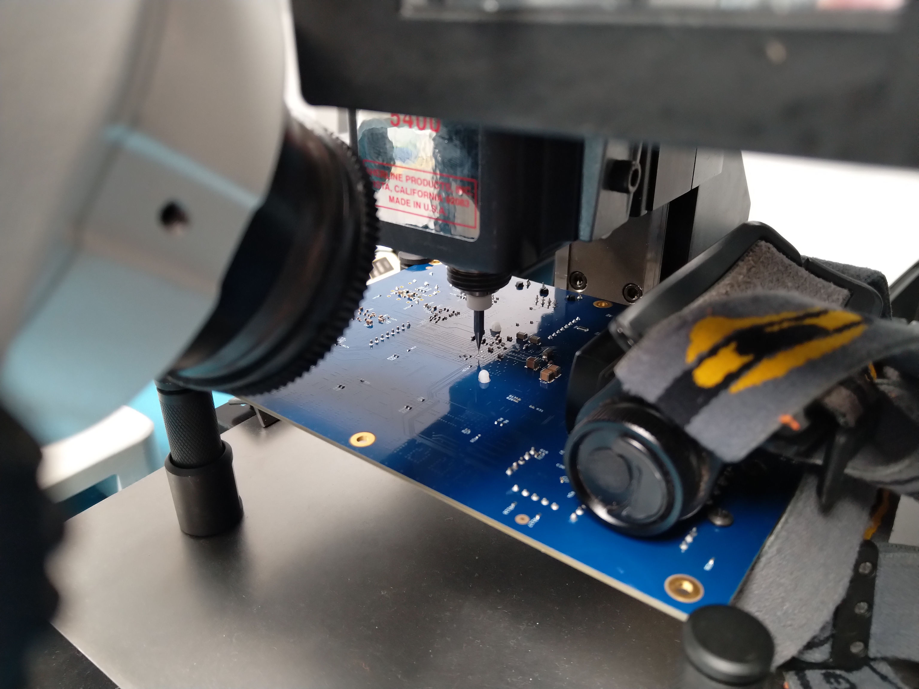
At this point there was nothing left to do but start drilling.
The overall setup was very similar to a dual-beam SEM/FIB scaled up by a few orders of magnitude and rotated: milling column coming in from the top, and imaging column at a ~45 degree angle for in-process inspection. And using a vacuum system (aka a shopvac) for removing debris from the milled cavity. No fancy secondary ion mass spectrometer is needed for endpoint detection though, you can just see the swarf change from white fiberglass to shiny red copper when you hit a metal layer.
Just like with a dual-beam, this sort of work requires making an angled cut to allow the angled imaging path to see the work area of the mill. I decided to orient the board in the canonical CAD orientation and come in from the south side, parallel to the JTAG traces. As long as I kept the cavity centered and not more than around 750 μm wide, there was no real danger of hitting the JTAG lines. The angled cut was more tricky as I had a VCCO via 1mm south of the work area that I needed to keep intact from L1 to L5 (but back-drilling it from L6 to L10 wouldn’t hurt anything), so I had to pay careful attention to depth as I approached this area.
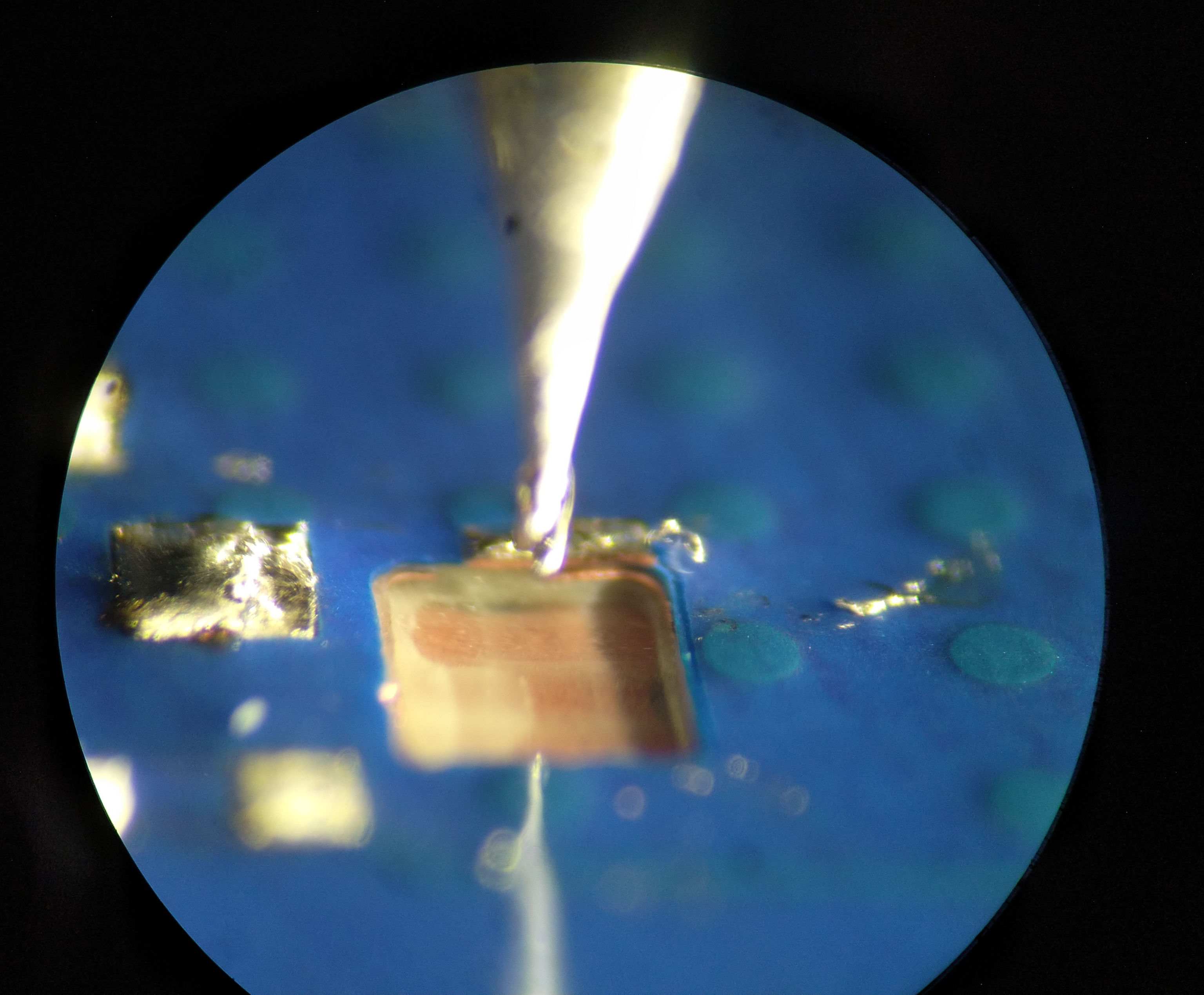
It worked perfectly. After about an hour of very careful machining, periodically stopping to unmount the board and look at it from different angles under the nice microscope, I saw the back side of the target BGA land coming into view, still under around 50 μm of laminate but clearly visible after adding a drop of IPA (a little trick I’ve learned when doing rework: it soaks into the resin and fills the gaps between the glass strands, acting to match the refractive index better and making it more transparent with less scatter)
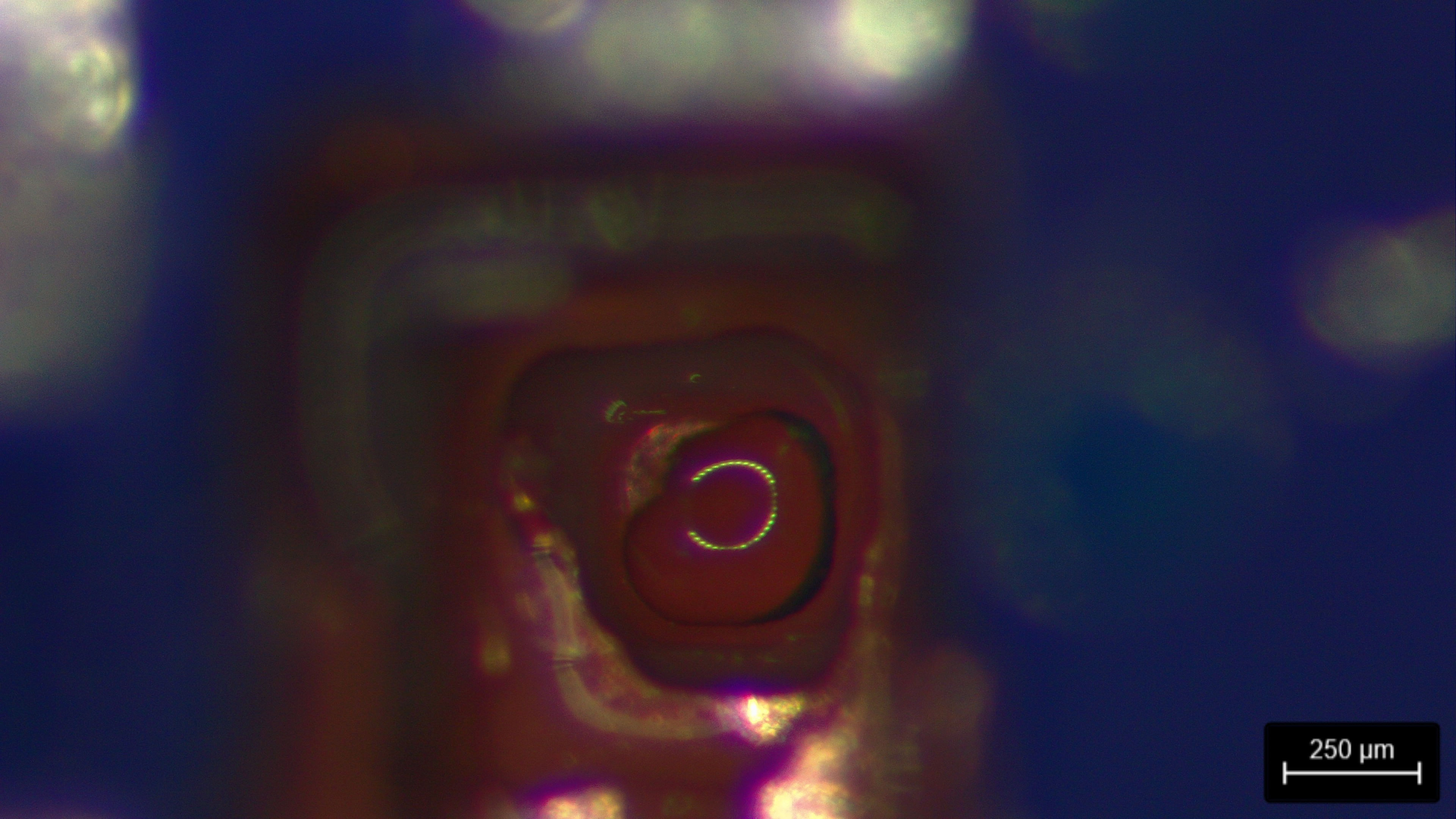
The only thing left to do was a final plunge cut to expose a 250 μm circle of bare copper to solder to. In this view you can clearly see how the milled cavity gets smaller and smaller as the target area approaches. This is rotated 180 degrees from canonical (south in CAD view is up in this image). Note the VCCO via barrel terminating at L5, then L4 ground plane visible slightly below it. The L2 ground plane is barely visible at the 7 o’clock position of the final hole.
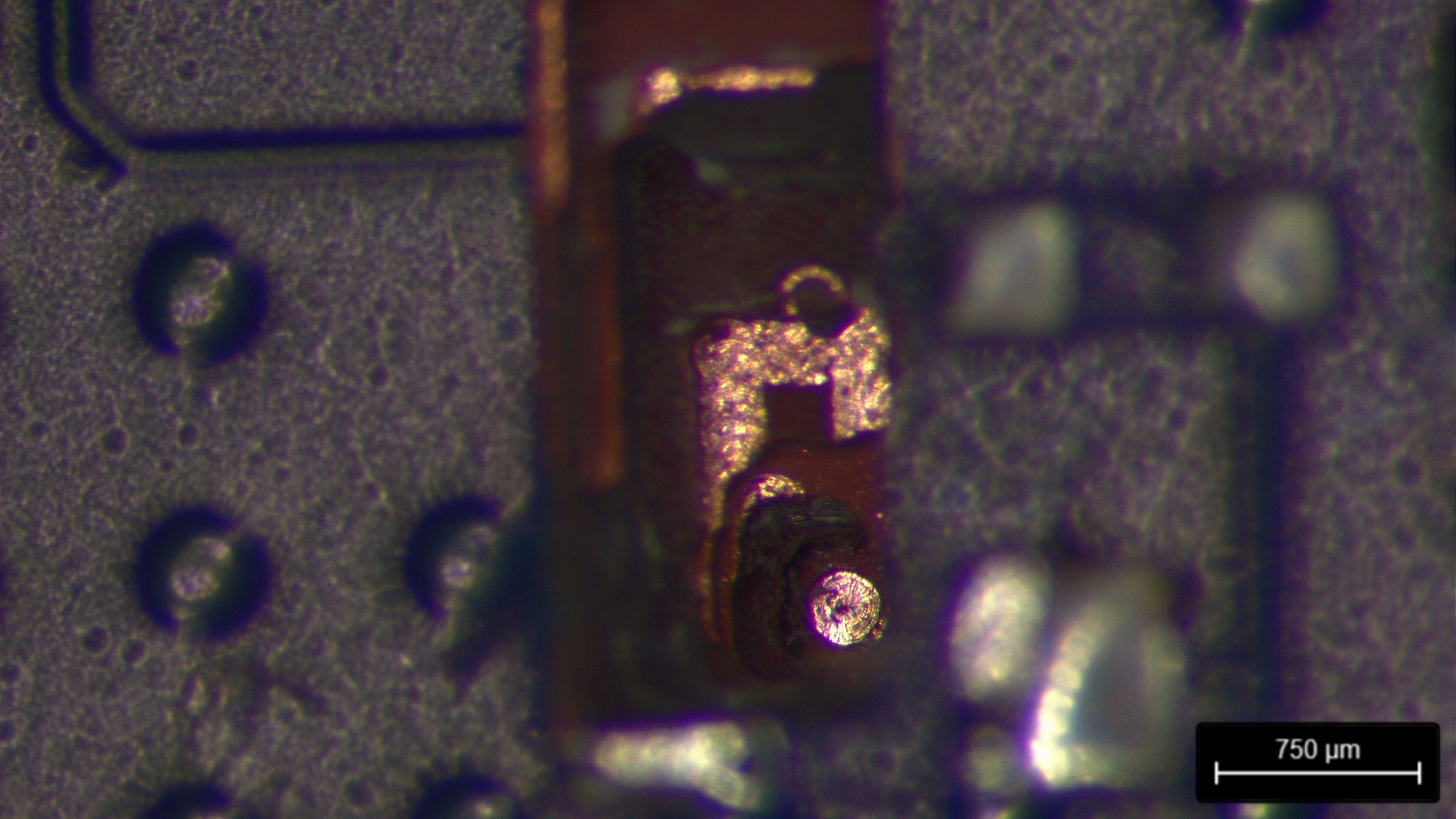
I did a final check for shorts and everything looked good. The only thing left to do was solder it up (not trivial, given that I’m trying to hit a 250 μm diameter target at the bottom of a 1.6mm deep hole).
After a few minutes of contorting myself trying to get a 100 μm conical soldering tip and a 125 μm bare copper wire positioned at the bottom of the hole while also angling the board enough that I could see under a microscope, I managed to get the wire securely attached.
Once that was done, I reconnected the VCCINT remote sense input, added a new series terminator to the CS# signal, put the removed decoupling capacitor back on its new slightly-smaller footprint, and tacked down all the wires with UV glue so they wouldn’t move around.
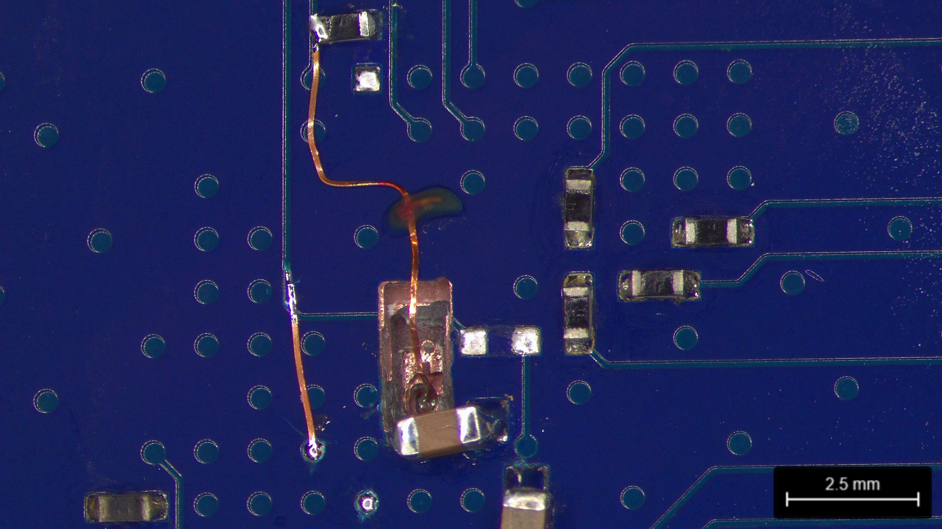
After verifying the board was electrically functional and I could program the flash and boot from it, I went back and flooded the whole area with UV cured conformal coating to lock everything in place permanently.
Chassis design and assembly problems
I went with a custom 1U enclosure from ProtoCase, designed using their free ProtoCase Designer software.
I have very mixed feelings about it: it has a lot of convenient templates and integrations with their standard pems and printing processes, and runs on Linux (a rarity in the proprietary CAD world). But it’s also a custom file format to lock you into their service, and if you import a couple of moderately complex STEP models of PCBs it slows to a crawl. I’ll probably keep using it for now, as the free tools don’t seem to be up to the task for complex sheet metal work and I don’t want to buy SolidWorks or something and set up a Windows VM for it.
My original plan had been to use their standard 1U folded sheet metal design, but I discovered too late, after boards were ordered, that it wasn’t going to work due to the 5mm corner mounting holes being inside the keepout area for the rear bend. I went with an extruded aluminum design, which let me salvage the design but had several significant problems:
- The stock template has no rack ears (although it’s 1U high) and there’s no way to add them within their software. I had to pay an hourly fee for one of their engineering technicians to create a new template with ears and extruded sides.
- The top and bottom panels slide into the extrusions and are held in place by the front and back. This means you cannot take the top panel off, e.g. to access JTAG ports for debug, without also removing the front panel (wearing out the self-tapping screws’ holes and putting shear forces on any attached cables)
- The front panel is only attached at the edges, and can flex relative to the top/bottom panels by quite a bit.
I’m definitely not going to use this case design again, although I made it work for a one-off. All of my future projects will do chassis-PCB codesign and not order boards until the enclosure is finished enough that I’m confident everything will mate properly.
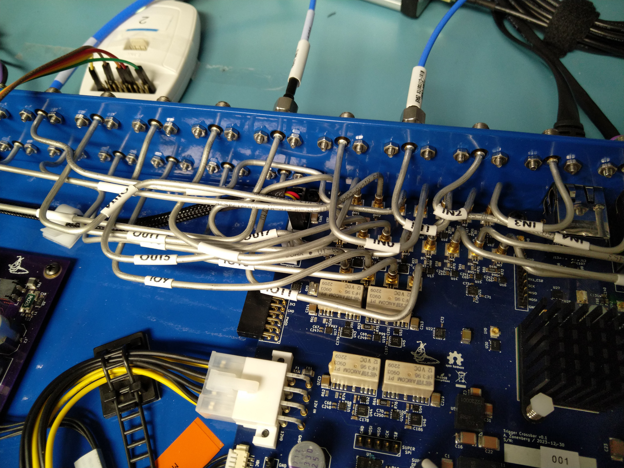
All of the front/rear panel coaxial ports connect to the logic board using custom sized SMA-to-SMPM semirigid cables. I went with semirigid to ensure the best possible repeatability of the trigger path delays, but it was likely overkill. It also made chassis assembly an absolute nightmare even with the custom 3D printed bending jigs I made… I’m never doing this again. Either flexible cables, hand-formable cables, or a much lower density design with semirigid that I have more space to route.
The biggest problem was that the SMAs bolted to the outside of the chassis, meaning that I had to pre-bend the cables, then thread the SMPM end in through the hole in the chassis, then try to snake the SMPM in through all of the previously installed cables. Lesson very painfully learned: I did get it fully assembled in the end, but I would never build a second unit like this.
I also had slightly oversized some of the cables thinking that this would be better than undersizing, but in many cases this led to extra slack that I had to remove by U-bends and such, adding to the tangle.
Front panel
The front panel has a STM32L431 and an I2C I/O expander to drive two rows of LEDs, showing pulse-stretched trigger input and output state. Four additional pairs of LEDs show the direction of the bidirectional ports, and a small e-paper display shows system health and status information.
I may have gone slightly overkill with the stitching vias on the board, but I’m so used to high speed designs that it’s a hard habit to break. I used an 0.5mm BGA package for the STM32 as a test to see if I could make it work on OSHPark, but probably would have just gone with the 48-QFN if this was a “real” product since there was absolutely no point in using a fine pitch BGA here.
This was my first time using e-paper and I initially had specced a white/black/red panel thinking I could use the red to denote error states or something, but quickly realized the error of my ways: the tricolor panels have a very very slow refresh rate and are really only suitable for signage, not user interface type stuff. Luckily Pervasive Displays made a pin- and mechanically-compatible B&W fast refresh display, so I swapped that in.
After spending a little while figuring out the not-great documentation for the panel controller and baking a few bitmap fonts into the STM32 firmware, I got it displaying some pretty system health stats: Ethernet link speed, IPv4/6 addresses, unit serial number, firmware timestamps for the FPGA and MCUs, input and output voltage/current/power for the IBC, temperatures at four points in the system, and fan speed.
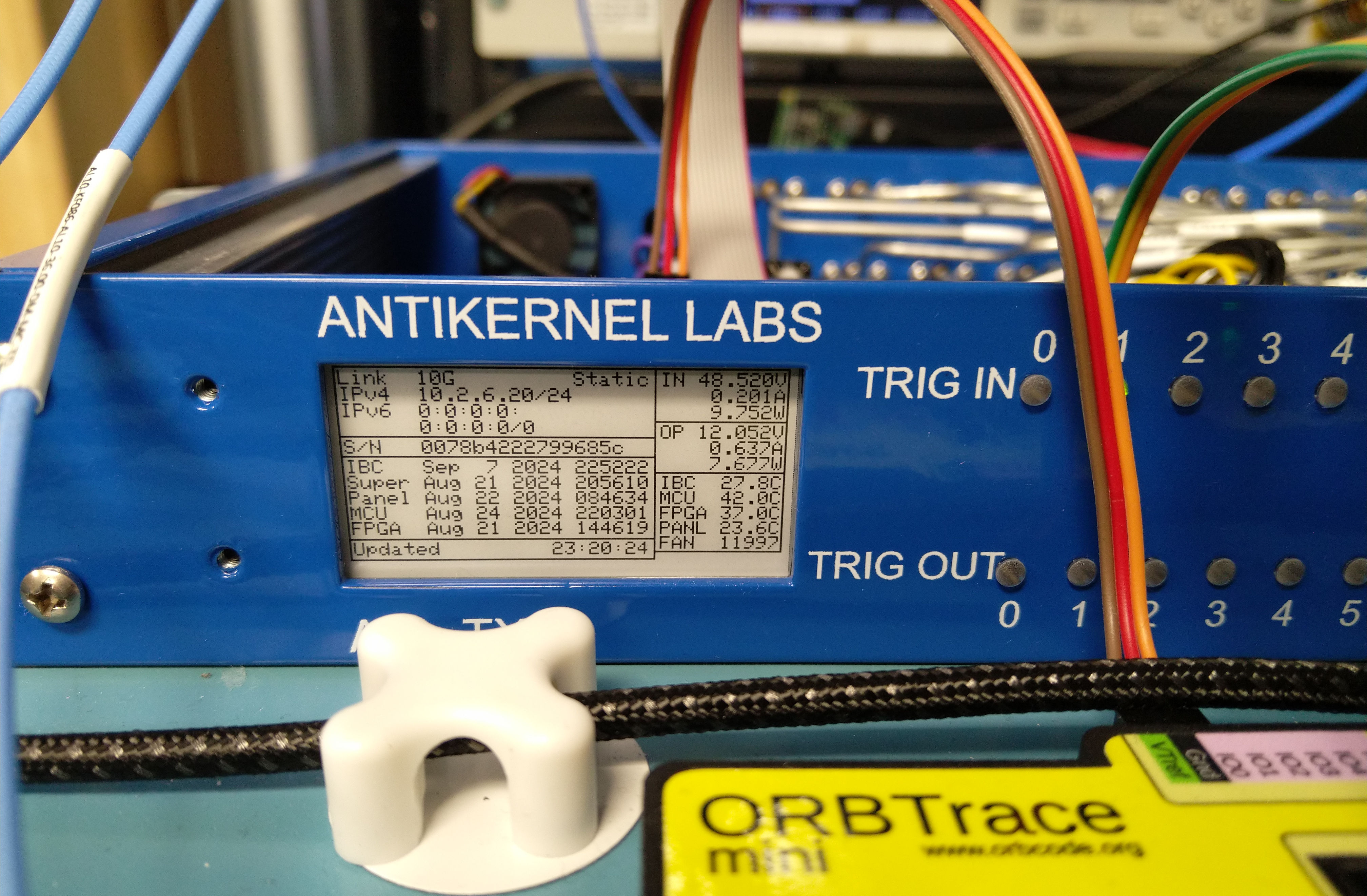
I also swapped the original first-generation IBC shown in the build photos with my second-generation MYC0409 based version to improve power efficiency, at which point the hardware was essentially done.
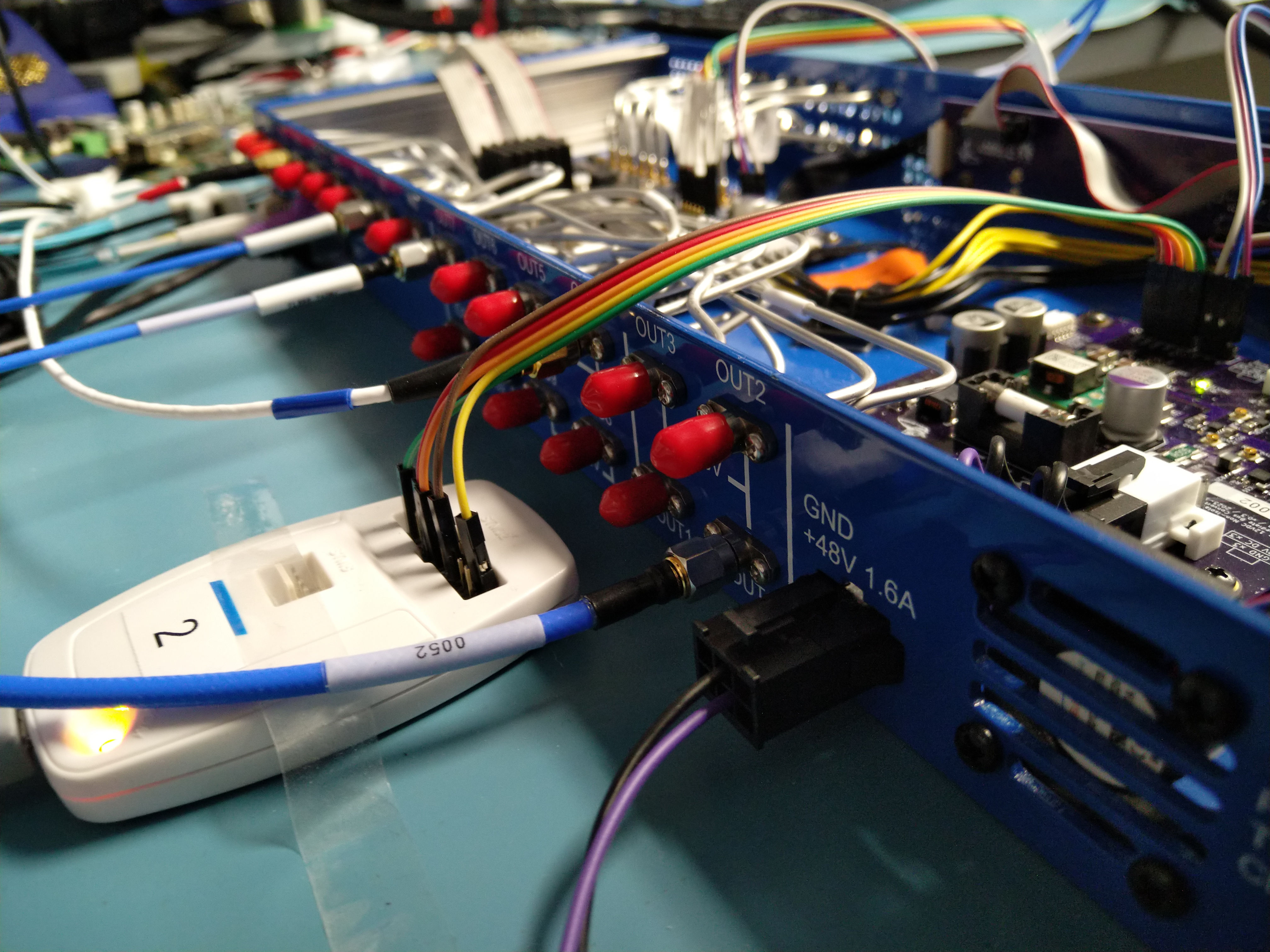
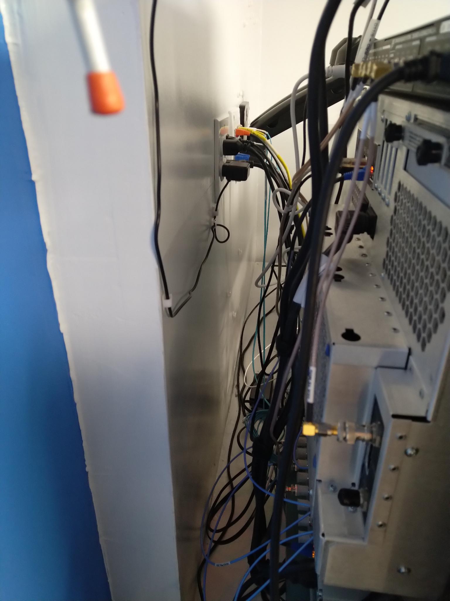
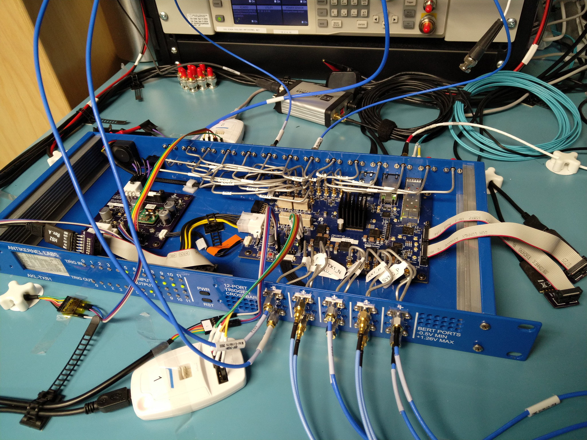
The unit is now mounted on one of my 19” benchtop racks and cabled to most of my instrumentation (I have a few more cables to run still but the main oscilloscopes and such are connected). I left the top off because I still have some firmware tweaks to do, so I need to be able to get JTAG/SWD dongles in to debug it.
Operation
The crossbar has two remoting interfaces: SSH and SCPI.
SSH
The SSH interface is mostly used for low level configuration and setup - managing keys for administrative access, forcing refreshes of the front panel LCD, displaying hardware sensor values, setting the NTP server IP address, etc.
It’s also used for firmware updates via SFTP. This is a somewhat unconventional DFU flow but I quite liked it:
- To flash the FPGA, SFTP a .bit file to /dev/fpga and it will be directly written to QSPI flash on the FPGA
- To flash the front panel or logic board MCU, SFTP an ELF binary to /dev/mcu or /dev/frontpanel. The ELF will be parsed live by the SFTP server and any PT_LOAD program headers in the flash address range are then written to flash. This is implemented in a single-pass streaming flow which requires a specific construction of the ELF (ELF header then program header table then program headers in linear address order) however all sane ELF generators like the GNU linker produce binaries that follow this. If you try to flash with a pathological ELF hand crafted in a hex editor and brick things, that’s on you :P
- Supervisor and IBC MCUs are not field updateable because they were (at the time) STM32L031 based and lacked the flash for a bootloader. IBC is now STM32L431 based so adding a bootloader is possible, but I can’t see any reason I’d want to OTA the power supply so I’ll probably just JTAG it if I ever need to patch.
Code signing support could be added to this flow easily (basically just mark the image as non-bootable in some way until you’ve checked the signature, then clear the flag once you’ve verified it). For the near term though, I trust that anyone with a valid administrative SSH key on the device is an authorized admin and can flash arbitrary code. Since that’s only me, it’s fine for now.
But since I have a curve25519 acceleration block in the FPGA already I’ll probably prototype a signing flow at some point just to have it available for future projects; I can always turn it off. The basic concept is to add an extra .signature section in the linker script that will be filled with 0x00 padding at link time, then a signing tool run post-link will hash the contents and headers of all data to be written to flash, sign with the curve25519 key, and overwrite .signature with that.
Signing the FPGA bitstream would be even simpler, just sign the entire .bit and append 32 bytes of signature to the end. The bitstream can be made unbootable by writing a dummy bitstream to the first flash sector containing an invalid CRC and a DESYNC command until the verification is done, then erasing this and writing the actual first sector bitstream content at the very end. This will require one flash erase block (typically 4 kB) of scratchpad buffer in the bootloader but not an entire bitstream worth of RAM, enabling a fly-by update flow at the cost of a second program/erase cycle on that one flash sector which is probably OK.
SCPI
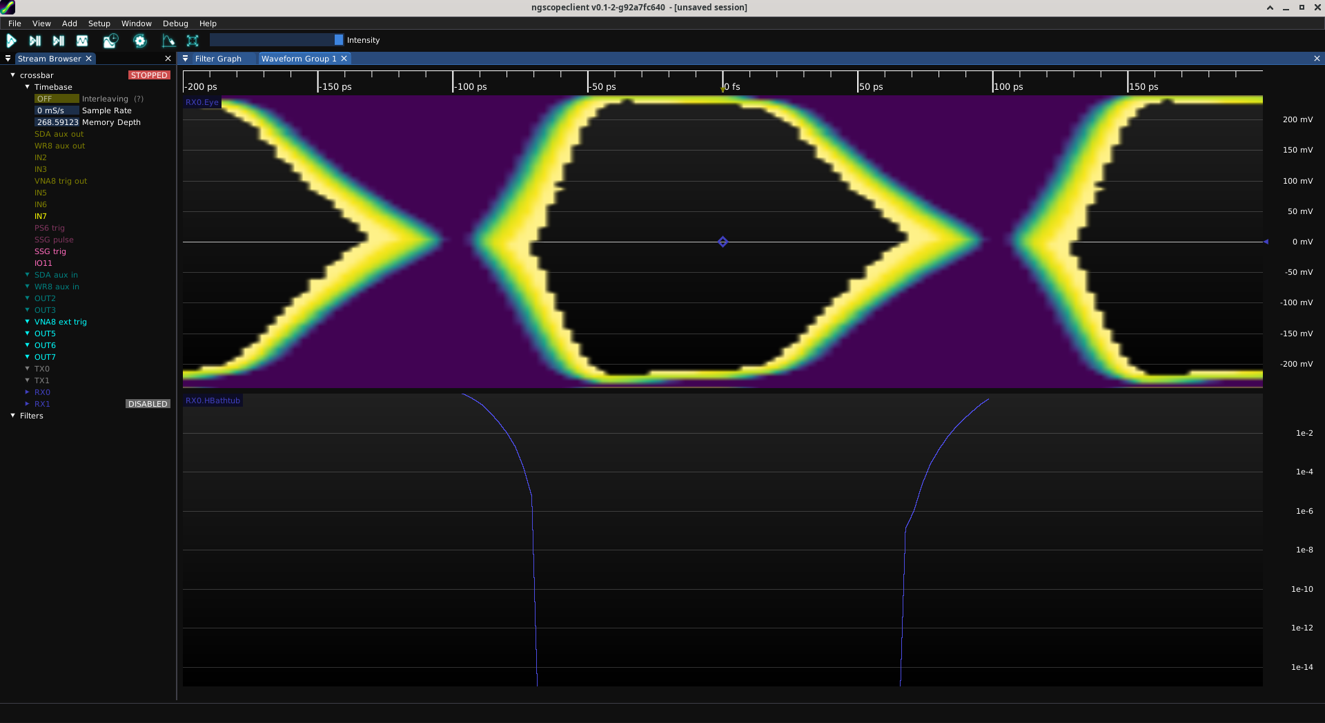
The SCPI interface is the primary remote control interface for application layer access to the crossbar. It provides a standard SCPI-compliant *IDN? command a well as custom commands for controlling the actual crossbar matrix, setting input thresholds and output levels, and accessing the BERT.
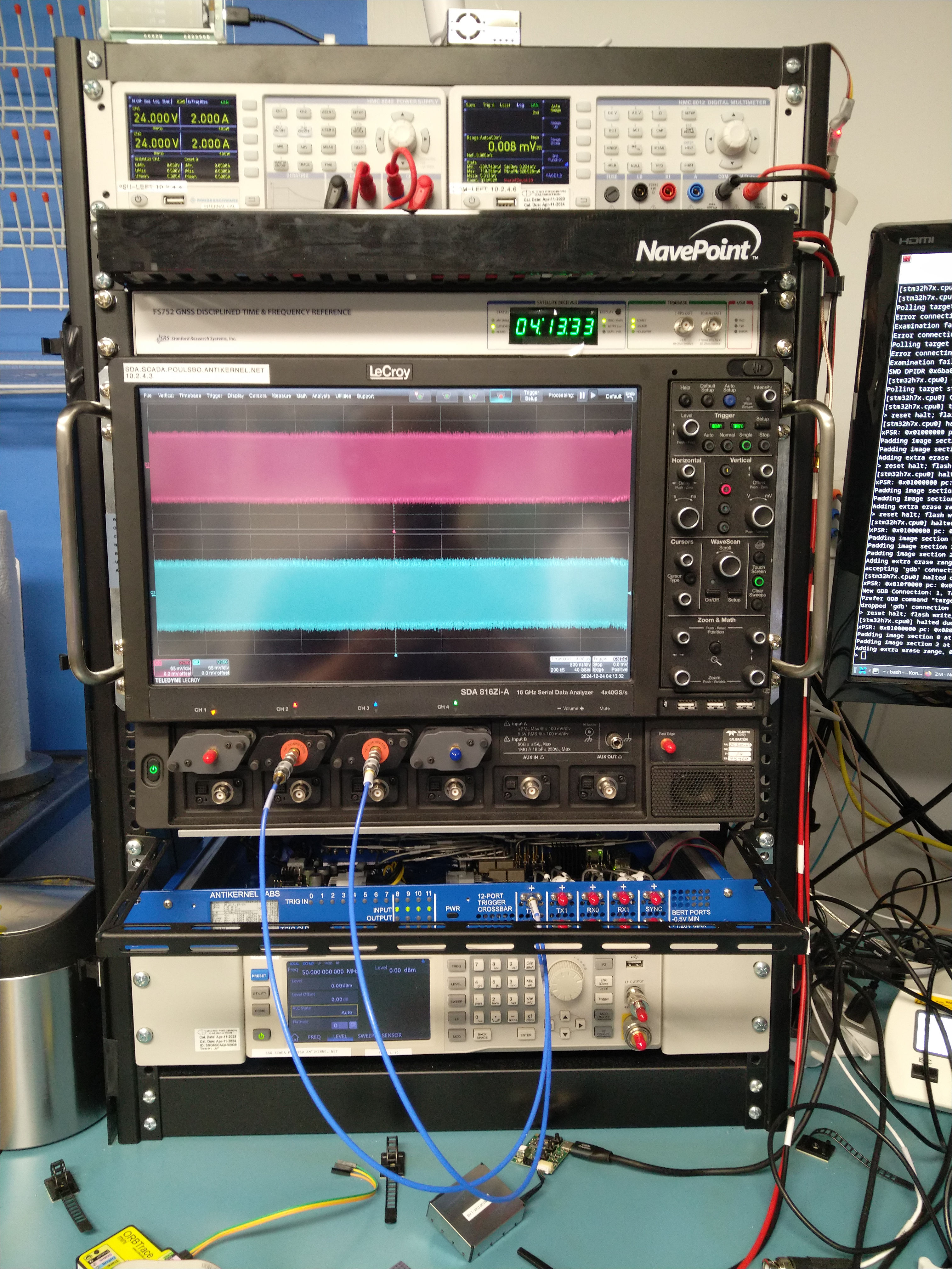
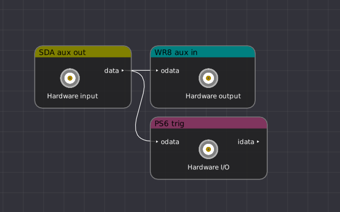
Crossbar paths can be configured in ngscopeclient by drawing connections in the filter graph from source port to sink port.
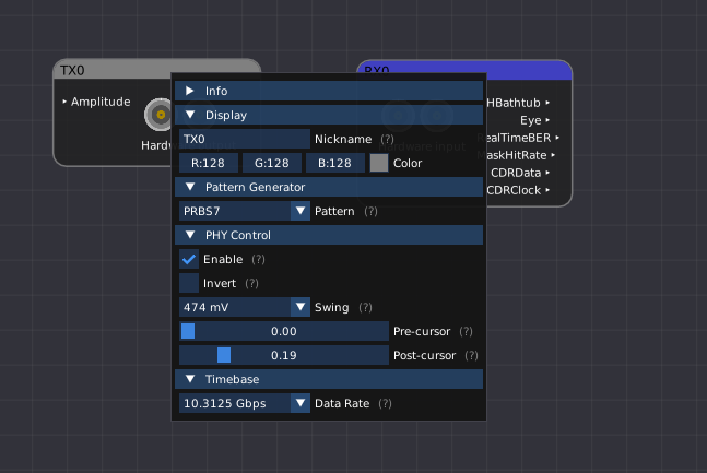
The BERT works pretty much like any other BERT supported by ngscopeclient. You can configure TX/RX bit rate, inversion, PRBS pattern or custom arbitrary pattern, NRZ baud rates from 625 Mbps to 10.3125 Gbps, etc. TX-side swing and pre/postcursor equalizer taps are also easily controlled from the channel properties dialog.
There’s still a few things I want to tweak. RX side equalization is currently fixed until I figure out how to properly tune the 7 series GTX receiver via the DRP. I haven’t implemented long-duration single point BER measurements, oversampling density plot mode, or offset sampling single-point scans.
The BERT inputs also contain an incomplete “CDR-based logic analyzer” feature. Essentially the raw GTX output is fed through 8b/10b or 64b/66b decoders and into a pattern matching block; once the requested trigger event is seen the LA will trigger and capture about a megapoint of raw line coded serial bits into block RAM then output to ngscopeclient as a waveform.
Eventually I want to finish building out various pattern triggers as well as integrating the CDR block with the trigger crossbar proper, such that a CDR pattern match can trigger an oscilloscope or other instrument.
The current gateware also provides a fixed 10.3125 Gbps PRBS-31 on the front panel “sync” port although I will likely make the baud rate and polynomial configurable at some point (basically a third output-only BERT channel). The intended use here is a deskew reference signal for use with ngscopeclient’s multi instrument sync feature, allowing the cross-trigger delay between multiple instruments to be automatically calibrated out.
Conclusions
This was my first large, standalone, rackmountable, network connected project that I’ve taken to something resembling completion in a long time (although I’m sure I’ll be continuing to poke at firmware for some time since the feature set isn’t quite where I want it). I learned a lot of things not to do, ranging from PCB design to mounting hole positionining to the awful OCTOSPI.
But it’s a useful tool I work with in my lab on a regular basis, and proved out a lot of software and hardware building blocks and techniques that I plan to use in many of my future projects, such as the Ethernet switch.
Like this post? Drop me a comment on Mastodon